
The IMPATT diode (Impact ionization Avalanche Transit-Time) is one which is used in high frequency applications and is a high power diode. This type of diode is used in microwave devices. In the frequency range of 3- 100GHz they can operate. The diode like n + pip+ , p+ n n+, p+ n n+ abrupt junction and p+ in+ diode are its basic types. The high level of doping is indicated by + sign here.
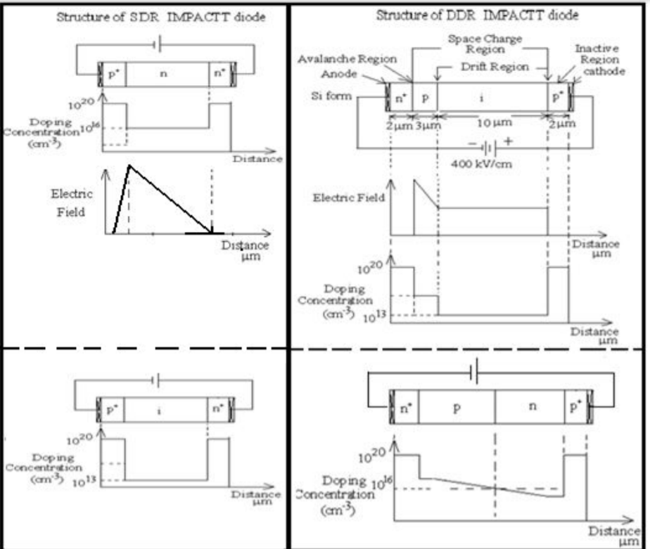
The SDR (Single Drift Region) and DDR (Double Drift Region) are the two types of IMPATT diode.
- Ga, Si, GaAs or InP are used for manufacturing IMPATT diodes. GaAs has high efficiency and operating frequency as well hence it is used mainly for manufacturing IMPATT. GaAs also has the least noise figure. But it has higher manufacturing cost than Silicon.
- They are mainly used in low-power radar systems and alarms as they have high power capability.
- These diodes generate phase noise because of the statistical nature of the avalanche process , setting a major drawback for this diode.
Operation
The diode produces high current upon the application of high voltage of range 400kV/cm. These diodes are manufactured such that they can withstand under such high voltage. When diode biased with such a high value of voltage results in flow of current due to minority carriers.
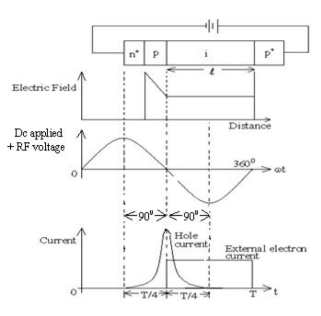
The phenomenon of impact ionization is responsible for the high flow of charge carriers i.e electrons and holes as a large number of the charge carriers are generated due to the application of RF voltage. The process is explained below in detail
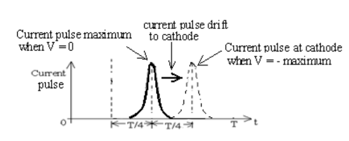
- During the positive RF cycle voltage is exceeded because of these additional carriers. During the entire process avalanche multiplication takes place. Avalanche is a cumulative process and not an instantaneous process. When the RF voltage across the diode is zero and goes negative the current pulse reaches its maximum value. The voltage and current are 90 degrees out of phase.
- As the diode is reversed biased the current pulse which is at the junction cannot stay there. Therefore, in a high dc field the current flows to the cathode due to the reverse biased condition. Depending upon the thickness of the highly doped n+ layer the time taken by the pulse to reach the cathode is estimated. The current arriving at the cathode is managed to have a phase difference of 90 degree by adjusting the thickness of the drift space. So now both voltage and current have a phase difference of 180 degrees.
Interested in learning about similar topics? Here are a few hand-picked blogs for you!
- Basic Logic Gates
- What is ALOHA?
- Working of SMPS
- What are PLCs? https://vepga.org/contract-materials/
- Working principle of Stepper Motor