
When a semiconductor is doped such that half the portion is doped with the trivalent impurity (Al, Ar, Bi) and the other half is doped with pentavalent impurity (B, P) then the junction formed is known as PN junction diode.
The basics of these semiconductors is discussed in this section.
n-Type semiconductors
The pentavalent impurities are added so that the number of electrons in the conduction band of intrinsic Si. These are atoms with five valence electrons such as
i) arsenic (As)
ii) phosphors (P)
iii) Bismuth (Bi)
iii) Antimony (Sb)

- As we see that the pentavalent impurity antimony (Sb) is added in the silicon crystal Each pentavalent atom forms covalent bonds with four adjustment silicon atoms, leaving one extra electron.
- They are called donor atoms because these pentavalent atoms give electrons. Majority and minority carriers: A type here means negative charge of an electron. Hence, making electrons as the majority carriers. Hole in an n-type material are called minority carriers
p-Type semiconductors
The trivalent impurities are added in order to increase the number of holes in intrinsic Si. These are atoms with three valence electrons such as
i) Boron(B)
ii) Indium (In)
iii)Gallium (Ga)

- The impurity atom boron is added to the trivalent impurity atom in a silicon crystal structure.
- The trivalent impurity can be added to the intrinsic silicon as per the requirement of the number of holes.
- A Hole created by the doping process is not accompanied by a conduction (free) electron.
- As the trivalent atom can take the place of an electron it is called an acceptor atom.
Formation of PN junction diode
A PN junction diode is basically formed by fusing p type and n type semiconductors.


Biasing
There are two of connecting a diode with an external ac supply. The diode can be either in forward bias condition or in reverse bias state.
Forward Biased
I forward bias state after applying dc supply the anode is now at higher potential and the cathode at the lower potential. The figure below helps to understand the connections.


- When the supply voltage increases the threshold potential of the diode it will conduct.
- Since the p terminal of the diode is connected to the positive terminal of supply the holes are repelled and pushed towards the N side.
- Similarly the N side of the diode is connected to the negative terminal which repels the electrons and pushes them towards the P side.
- This then causes the current to flow in the PN junction diode.
- Hence, the width of the depletion region in forward bias is reduced in this biasing.
- The diode acts as a short circuit in this biasing and also allows conduction in the ideal case.
Reverse Biased
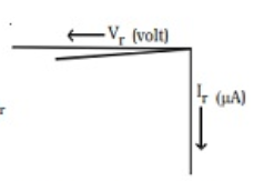
In this when dc supply is connected then the anode is connected to lower potential and cathode to the higher potential. The figure below helps to understand the connections.

- Since the p terminal of the diode is at the lower potential of supply the holes are moving towards the N side.
- Since the N terminal of the diode is at the higher potential of supply the electrons are moving towards the P side.
- This causes very less amount of the reverse current to flow in the PN junction diode.
- Hence, the width of the depletion region in reverse bias is increased in this biasing.
- Therefore the diode acts as an open circuit in this biasing and does not allow conduction in the ideal case.
Interested in learning about similar topics? Here are a few hand-picked blogs for you!
- Basic Logic Gates
- What is ALOHA?
- Working of SMPS
- What are PLCs? https://portal.firststeps.edu.pk/
- Working principle of Stepper Motor