
There are three types of transistor configurations CB (common base), CE (common emitter), and CC (common collector). In the below section we will learn in detail about the CE CB CC transistor configurations along with their input and output characteristics.
Common Base (CB)
The notation and symbols of pnp and npn transistors are given below:

- Here the base is common to both the input and output sides of the configuration.
- The flow of holes will govern the direction of current.
- Hence, Ic = Ib + Ie
- Where Ic, Ib, Ie are the collector, base and emitter currents respectively.
- The graphical symbol of the PNP common base configuration is

- The arrow in the above symbol shows the direction of emitter current in the device.
- Now, to study the behavior of the device we require two characteristics:
Input Characteristic Curve of CB
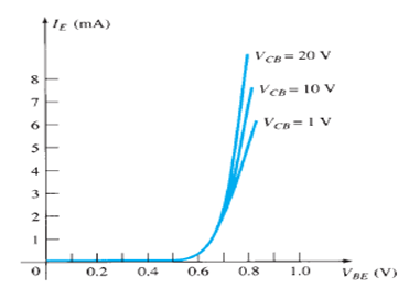
- It is the relation between the input current IE to the input voltage VBE for various levels of output voltage VCB.
- It is also known as driving point characteristics.
Output Characteristic Curve of CB
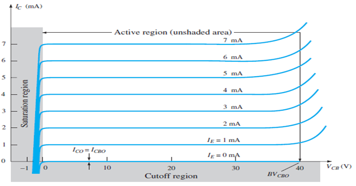
- It is also the relation between the output current IC to the output voltage VCB for various levels of input current IE.
- Also known as the collector set of characteristics.
- Therefore, it has three basic regions:
Active Region
- Here, the base-emitter junction is forward biased and collector-base junction is reverse biased.
- Since the input current IE increases above zero, output current IC increases to a magnitude equal to IE as determined by the basic transistor current relationship.
- So, the first approximation determined by the curve is
IC ≈ IE
Cut-off Region
- It is defined as the region where the collector current IC is equal to 0A.
- Here, the base-emitter junction and the collector-base junction both are in reverse bias.
Saturation Region
- It is the region that lies towards the left of VCB = 0V.
- Since the base-emitter junction and the collector-base junction both are in forward bias.
Common Emitter Configuration (CE)
- The notation and symbols of npn and pnp transistors are given below:
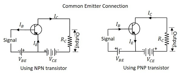
- In the above figure all the currents are shown in their actual conventional directions.
- The current relation developed earlier is still applicable,
- IE = IB + IC
- Where IE , IB , IC are the collector, base and emitter currents respectively.
- The graphical symbol of the PNP common emitter configuration is

- Now, to study the behavior of the device we require two characteristics:
Input Characteristic Curve

- It is the graph between the input current IB to the input voltage VBE for a range of values of output voltage VCE.
- Note that the magnitude IB of is in micro amperes and that of IC is in milli amperes.
Output Characteristic Curve

- It is the graph between the output current IC to the output voltage VCE for a range of values of input current IB.
- The three basic regions are:
Active Region
- Here, the base-emitter junction is forward biased and collector base junction is reverse biased.
- These are the same conditions that existed in the active region of the common base configuration.
- This can also be employed for voltage, current or power amplification.
Cut-off Region
- Here IC is not equal to zero when IB is zero.
- For linear amplification purposes, it is defined as IC = ICEO.
- The region below IB = 0µA is to be avoided for undistorted output signals.
- When the transistor is used as a switch, the condition should be ideally IC = 0mA for a chosen VCE voltage.
Saturation Region
- It is the region that lies towards the left of VCE = 0V.
Common Collector Configuration (CC)
The notation and symbols of npn and pnp transistors are given below:

- In the above figure all the currents are shown in their actual conventional directions.
- It is used for impedance matching purposes as it has high input impedance and low output impedance.
- It can also be designed using common emitter characteristics.
- Then output characteristics of a common collector is the same as that of common emitter configuration for all practical purposes.
- Then output characteristics are a plot between IE versus VCE for all values of IB.
- The input current of the common collector is also the same as that of common emitter configuration.
- Here the region of operation will ensure that maximum ratings are not being exceeded and also output ratings have minimum distortion.

- The characteristics specifying the minimum VCE that can also be applied without entering the non-linear region is the saturation region.
- Then maximum power dissipation is given by, https://www.bmich.com/news/
P = VCE. IC