
- The MOSFET (metal-oxide-semiconductor field-effect transistors) are of two types: PMOS (p-type MOS) and NMOS (n-type MOS).
- A new type of MOSFET logic is made combining both the PMOS and NMOS processes and is called complementary MOS (CMOS).
- CMOS stands for “Complementary Metal Oxide Semiconductor”.
- It is one of the most popular technologies in the chip design industry and is used today to form integrated circuits for various applications.
- Computer memories, CPUs and cell phones make use of this technology due to various advantages. This technology uses both P and N channel semiconductor devices.
Construction
The CMOS is a logic made with PMOS and NMOS. The explanation of symbol both symbol is below.
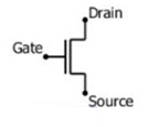
NMOS
A p-type substrate is used which has n-type source and drain diffused on it. Here, the majority carriers are electrons. When a high voltage is applied to the gate, the NMOS conducts and when low voltage is applied to the gate, it does not conduct. NMOS is faster than PMOS, as the carriers are electrons that travel twice as fast as the holes.
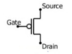
PMOS
P-MOS consists of P-type Source and Drain diffused on an N-type substrate. Holes are the majority carriers. When a high voltage is applied to the gate, the PMOS does not conduct and when a low voltage is applied, it conducts. These devices are more immune to noise than NMOS devices.
Applications
- Computer memories, CPUs
- For designing Microprocessors
- In the Flash memory chip designing also we use them.
- Used to design application specific integrated circuits (ASICs)
CMOS as an Inverter
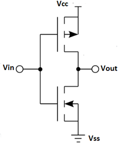
The inverter circuit as shown in the figure above. Also we already know, PMOS and NMOS form a CMOS.
The NMOS transistor has an input from Vss (ground) and also the PMOS transistor has an input from Vdd. Then the terminal Y is output. When input terminal A will have supply with a high voltage (Vdd) of the inverter, the PMOS becomes open circuit and NMOS switches OFF so the output will be pull down to Vss.
When a low-level voltage (<Vdd, ~0v) applied to the inverter, the NMOS switched OFF and PMOS switched ON. So, the output becomes Vdd or the circuit is pull up to Vdd.
| INPUT | LOGIC INPUT | OUTPUT | LOGIC OUTPUT |
| 0 V | 0 | Vdd | 1 |
| Vdd | 1 | 0 v | 0 |
Interested in learning about similar topics? Here are a few hand-picked blogs for you!
- What is ZigBee?
- Encoders and Decoders
- Working of UART https://museuboulieu.org.br/
- Classification of FFT
- Fourier Transform and its properties