
The electronic circuit which produces the samples of the input voltage and holds those values for a definite amount of time is the Sample and Hold circuit. The duration of time which it needs to generate the sampled data at the output is the sampling time. The sample and hold circuit can have sampling time between 1µs to 14 µs.
Since the capacitor charges to peak value when the switch is opened (during sampling) and maintains the voltage till the switch is closed. Therefore, the main component of this circuit is a capacitor. The time for which the circuit can hold the sample values is holding time.
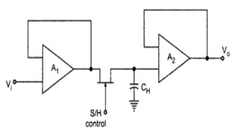
Need of Sample and Hold Circuits
When the value of analog input voltage is more than ±1/2 LSB the value of output voltage has an error. In order to generate accurate results it is necessary to hold the analog input voltage till the conversion is complete. On every sampling command the circuit samples and holds the output. The below illustration shows the output of a conventional S/H circuit.

The Analog Switch and holding capacitors are the main components of the sample and hold circuit.


Acquisition Time (tac)
The time required during sampling by the capacitor voltage to increase to a level which is close to the input voltage is the acquisition time. The RC Time Constant, slew rate of op-amp and value of maximum output current of op-amp are some of the factors which affect the acquisition time.
Aperture Time (tap)
When there is delay between the output tracking the input and initiation of the hold command is the aperture time. Due to the propagation delay through drivers as switches this delay occurs. If the hold command is initiated prior to the aperture time we can get accurate timing operation.
Aperture Uncertainty (∆ tap)
Since the aperture time varies for all the samples and is not same for all samples is the Aperture Uncertainty.
Hold Mode Settling Time (ts)
The initial time which is required by the output to settle within the specified error band is called as hold mode settling time.
Hold Step
Since there are chances of unwanted charge transfer between the switch and holding capacitor the value of capacitor voltage at the output is affected. When there is change in the output voltage from the required voltage is the hold step.
Feedthrough
In hold mode the parasitic capacitance can cause AC coupling. Hence, there can be change in the value of output voltage with respect to the change in input values. Then we call it as feedthrough.
Droop
The drop in voltage capacitor due to voltage drop in the holding capacitor drops known as Voltage Droop.
Advantages
- They help in analog to digital conversion by sampling the input voltage and holding it till the conversion is complete.
- The S/H are more useful in multichannel ADC where the need of synchronization is necessary. The S/H circuit samples all the signals from different channels at the same time.
- This S/H circuits reduce cross talk in multiplexed circuits.