Line Regulation = |

Line Regulation = |

Ripple Rejection = 20log [ |

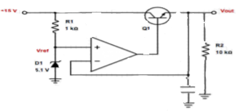
VB = Vout. The voltage at non inverting terminal at node A is Zener voltage VZ VA = VZ. Due to the concept of virtual ground VA = VB V0 VZ |
|
|

|
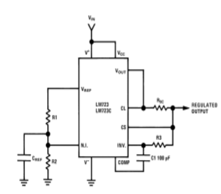
The difference between VN1 and output voltage V which is directly fed back to the inverting terminal is amplified by the error amplifier. The output of the error amplifier drives the ass transistor Q1 so as to minimize the difference between the NI and Inv input of error amplifier. Since Q1 is operating as an emitter follower
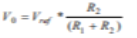
As we see V+ = +VCC, V- = GND, R3 = R1||R2. Then Vo = VNI Vo = 7.15xR2/(R1+R2) The typical value of reference voltage Vref is 7.15V. So that output voltage VO is always less than7.15V. By suitably designing the value of R1 and R2 the output voltage ranging from 2V to 7V can be built. |

|

Av = 1+ (Rf/R1) Output voltage gain is given as Av = 7.15(1+ Rf/R1) Key takeaways For high voltage regulation voltage gain is Av = 1+ (Rf/R1) Output voltage gain is given as Av = 7.15(1+ Rf/R1) |
|


