Unit - 6
Three phase DC-AC Converter
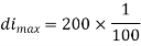
Q1) The separately excited dc motor in the figure below has a rated armature current of 20 A and a rated armature voltage of 150 V. An ideal chopper switching at 5 kHz is used to control the armature voltage. If La = 0.1 mH, Ra 1 , neglecting armature reaction, the duty ratio of the chopper to obtain 50% of the rated torque at the rated speed and the rated field current is?
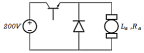
A1)
Given the rated armature current

As rated armature voltage
Also, for the armature we have
So, we get
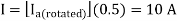

 rated field current
At the rated conditions,
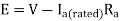
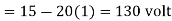
For given torque,

Therefore, chopper output 

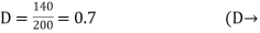 duty cycle)
Q2) The Voltage Source Inverter (VSI) shown in the figure below is switched to provide a 50 Hz, square wave ac output voltage Vo across an RL load. Reference polarity of Vo and reference direction of the output current io are indicated in the figure. It is given that R = 3 ohms, L = 9.55 mH. (i) In the interval when V0 < 0 and i0 > 0 the pair of devices which conducts the load current is? (ii) Appropriate transition i.e., Zero Voltage Switching ZVS /Zero Current Switching ZCS of the IGBTs during turn-on/turn-off is?
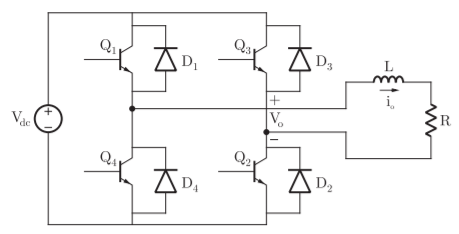
A2) (i) We consider the following two cases: Case I: When Q Q1 2, ON In this case the +ve terminal of V0 will be at higher voltage. i.e., V0 > 0 and so i0 > 0 (i.e., it will be +ve). Now, when the Q1, Q2 goes to OFF condition we consider the second case. Case II: When Q3, Q4 ON and Q, Q2 OFF: In this condition, -ve terminal of applied voltage V0 will be at higher potential i.e., V0 < 0 and since, inductor opposes the change in current so, although the polarity of voltage V0 is inversed, current remains same in inductor i.e. I0 > 0. This is the condition when conduction have been asked. In this condition (V0 > 0, I0>0), since, IGBT’s can’t conduct reverse currents therefore current will flow through D4 D3, until ID becomes negative. Thus, D3 and D4 conducts.
(ii) When Q4 Q3, is switched ON, initially due to the reverse current it remains in OFF state and current passes through diode. In this condition the voltage across Q3 and Q4 are zero as diodes conduct. Hence, it shows zero voltage switching during turn-ON.
Q3) In the 3-phase inverter circuit shown, the load is balanced and the gating scheme is 180c conduction mode. All the switching devices are ideal. (i) The rms value of load phase voltage is? (ii) If the dc bus voltage Vd = 300V the power consumed by 3-phase load is?
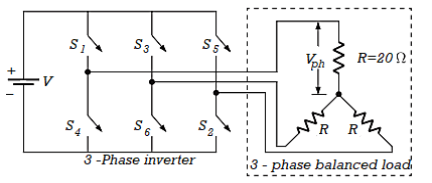
A3) For a three-phase bridge inverter, rms value of output line voltage is
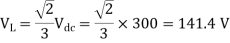

(ii) 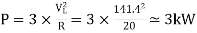
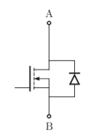
Q4) A three phase current source inverter used for the speed control of an induction motor is to be realized using MOSFET switches as shown below. Switches S1 to S6 are identical switches. The proper configuration for realizing switches S1 to S6 is?
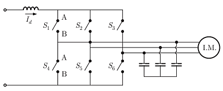
A4) The below figure allows bi direction power flow from source to the drive
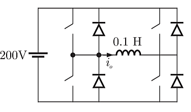
Q5) The Current Source Inverter shown in figure is operated by alternately turning on thyristor pairs (T1, T2) and (T3 T4). If the load is purely resistive, the theoretical maximum output frequency obtainable will be?
A5) In CSI let T3 and T4 already conducting at t = 0 At triggering T1 and T2, T3 and T4 are force cumulated. Again, at t= T/2, T1 and T2 are force cumulated. This completes a cycle.
Time constant =RC=4×0.5=2 sec
Frequency 
Q6) A single phase source inverter is feeding a purely inductive load as shown in the figure. The inverter is operated at 50 Hz in 1800 square wave mode. Assume that the load current does not have any dc component. The peak value of the inductor current i0 will be?
A6) Input is given as
Here load current does not have any dc component
Peak current occurs at (π/)

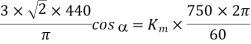
Q7) A three phase fully controlled bridge converter is feeding a load drawing a constant and ripple free load current of 10 A at a firing angle of 300. The approximate Total harmonic Distortion (%THD) and the rms value of fundamental component of input current will respectively be?
A7)
Total rms current 
Fundamental current 

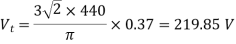
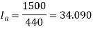
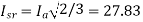
Q8) A three-phase, fully controlled thyristor bridge converter is used as line commutated inverter to feed 50 kW power 420 V dc to a three-phase, 415 V(line), 50 Hz ac mains. Consider dc link current to be constant. The rms current of the thyristor is?
A8) Given that 


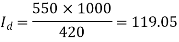
RMS Value of thyristor current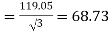
Q9) A three-phase, 440 V, 50 Hz ac mains fed thyristor bridge is feeding a 440 V dc, 15 kW, 1500 rpm separately excited dc motor with a ripple free continuous current in the dc link under all operating conditions, Neglecting the losses, the power factor of the ac mains at half the rated speed is?
A9) When losses are neglected
Here back emf with  is constant
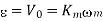
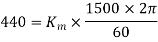


At this firing angle
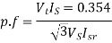
Q10) The triggering circuit of a thyristor is shown in figure. The thyristor requires a gate current of 10 mA, for guaranteed turn-on. The value of R required for the thyristor to turn on reliably under all conditions of Vb variation is?
A10)


Required value of 
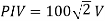
Q11) The circuit in figure shows a full-wave rectifier. The input voltage is 230 V (rms) single-phase ac. The peak reverse voltage across the diodes D1 and D2 is
A11)
Peak Inverse Voltage (PIV) across full wave rectifier is 

Q12) An ac induction motor is used for a speed control application. It is driven from an inverter with a constant V f / control. The motor name-plate details are as follows (no. Of poles = 2) VVf N :415 :3 :50 :2850 V Hz rpm Ph The motor runs with the inverter output frequency set at 40 Hz, and with half the rated slip. The running speed of the motor is?
A12)
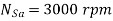
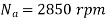
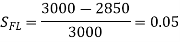
Where by  control
 new running speed of motor
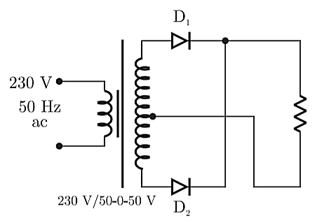
Q13) The circuit in figure shows a 3-phase half-wave rectifier. The source is a symmetrical, 3-phase four-wire system. The line-to-line voltage of the source is 100 V. The supply frequency is 400 Hz. The ripple frequency at the output is
A13)
Ripple frequency 
So, from  ripple frequency =1200Hz
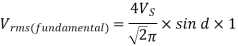
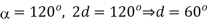
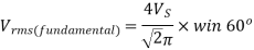
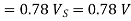
Q14) An inverter has a periodic output voltage with the output wave form as shown in figure
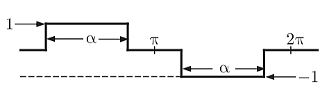
When the conduction angle, a = 1200, the rms fundamental component of the output voltage is?
A14)
RMS value of fundamental component
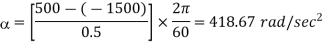
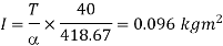
Q15) A variable speed drive rated for 1500 rpm, 40 Nm is reversing under no load. Figure shows the reversing torque and the speed during the transient. The moment of inertia of the drive is
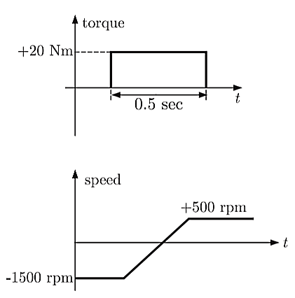
A15)


Q16) Compare various multilevel converters?
A16)
Sr. No. | Topology | Diode | Clamped Flying Capacitor | Cascaded |
1 | Power semiconductor switches | 2(m-1) | 2(m-1) | 2(m-1) |
2 | Clamping diodes per phase | (m-1) (m-2) | 0 | 0 |
3 | DC bus capacitors | (m-1) | (m-1) | (m-1)/2 |
4 | Balancing capacitors per phase | 0 | (m-1) (m-2)/2 | 0 |
5 | Voltage unbalancing | Average | High | Very small |
6 | Applications | Motor drive system, STATCOM
| Motor drive system, STATCOM | Motor drive system, PV, fuel cells, battery system |
Q17) Explain NPC and Flying capacitor type converters?
A17) The neutral point clamped converter [NPC] is shown below.
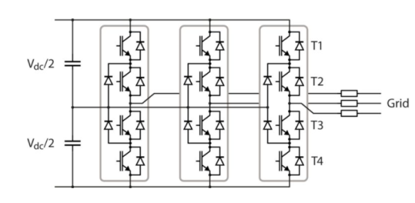
Fig 1 NPC converter
Each inverter consists of four transistors and they all can be controlled by 16 (=24) states. Out of these only 3 states can be used because other create short circuit on the DC link. The three states which are possible are Vdc/2, -Vdc/2 and 0V. The conductivity of transistor is shown below in the table.
T1 | T2 | T3 | T4 | Output voltage | Leg state |
ON | ON | OFF | OFF |  | P |
OFF | ON | ON | OFF | 0V | 0 |
OFF | OFF | ON | ON |  | N |
There are some modulation techniques used in NPC converter such as Carrier based PWM and space vector modulation (SV-PWM). More care is required in these inverters while balancing the voltage of the DC mid-point which cannot be achieved neutrally.
Flying Capacitor Converter
In this technique mainly capacitors are used in series and then clamped. The limited amount of voltage is transfer to electrical devices through these capacitors. There is no need of clamping diode in this type of multilevel inverters. The output voltage obtained is half of the input DC voltage. This is the main drawback of multilevel inverter. In order to balance the flying capacitor, it has switching redundancy within the phase. To control both active and reactive power they can be used. There are switching losses because of high switching frequencies.
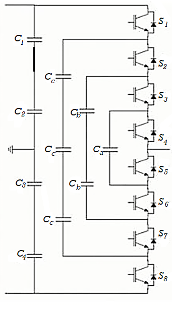
Fig 2 Flying capacitor multilevel inverter
They are used in IM control using direct torque control circuit. They are also used in static var generation. They also act as sinusoidal current rectifiers. We can perform both AC-DC and DC-AC conversion using these inverters.
Q18) Draw circuit of transistor based 3-phase Voltage Source Inverter and explain its operating modes?
A18) For high power applications, three phase voltage source inverters are preferred to provide three phase voltage sources in addition to that the magnitude, phase and frequency of voltages should be controlled.
The typical three-phase VSI topology is shown in fig below, and middle points of the inverter legs are connected to three phase RL load. There are the eight valid switch states which are given in Table. The switches of any leg of the inverter (S1 and S4, S3 and S6 or S5 and S2) cannot be switched on simultaneously. Because it would result in short circuit across the DC link voltage supply. Similarly, the switches of any leg of the inverter cannot be switched off simultaneously to avoid undefined states in the VSI and thus undefined ac output line voltages.
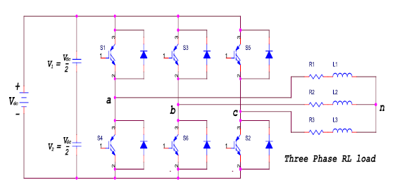
Fig:3 Power circuit of three phase voltage source inverter with RL load
Two of eight valid states (7 and 8) are called as zero switch states to produce zero AC line voltages. In this case, the AC line currents freewheel through either the upper or lower components. The remaining states (1 to 6 in Table) are called as non-zero switch states to produce non-zero AC output voltages. The resulting AC output line voltages consist of discrete values of voltages that are Vdc, 0, and - V dc for the topology shown in waveform figure below.
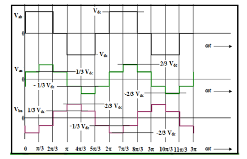
Fig:4 Output voltage waveform of three phase VSI
The pole voltages and output voltage waveforms obtained with respect to switching states from three phase VSI are shown in waveform. Analysis of three phase VSI is carried out in either 1200 mode or 1800 mode of conduction.
1800 conduction Mode
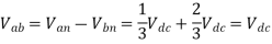
In this mode each switch turned on at every 600. Conduction of switches in each switching states, pole voltages measured at ‘a’ and ‘b’ and load voltage (Vab) are noted in the Table below.
State | Switching state | Output voltage | ||
 |  |  | ||
1 |   |  | 0 |  |
2 |   |  |  | 0 |
3 |   | 0 |  |  |
4 |   |  | 0 |  |
5 |   |  |  | 0 |
6 |   | 0 |  |  |
7 |   | 0 | 0 | 0 |
8 |   | 0 | 0 | 0 |
Table: Switching states and output voltages of three phase VSI
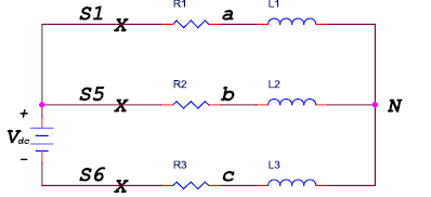
Fig:5 Equivalent circuit representation at 0≤ωt≤π/3
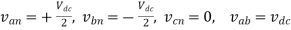
With reference to above figure, it is clear that for 0≤ωt≤π/3, the power switches S6, S1 and 5S conduct and it will represent the equivalent inverter and load circuit during the above time interval. In such cases, when the load is a balanced one, it is easy to find the phase voltages for each phase and that can be given as


And 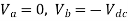
1200 conduction mode
In this type of control, only two transistors conduct at the same time such that each transistor conducts for 120˚ and remains OFF for 240˚. This means that only two transistors remain “ON” at any instant of time.
The conduction sequence of the transistors is: 1,6-1,2-2,3-3,4-4,5-1,6-1,2-2,3
During mode-1 for 0 ≤ ωt ≤ π/3 transistor 1and 6 conduct:
During mode-2 for π/3 ≤ ωt ≤ 2π/3 transistor 1and 2 conduct:
During mode-3 for 2π/3 ≤ ωt ≤ π transistor 3 and 2 conduct:
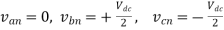
Fig:6 Voltage waveform in 1200 conduction mode
Mathematical analysis of 120˚ Mode inverter
The rms value of the output voltage waveform of 120˚ mode inverter for phase-a can be obtain as,
The line-to-line voltages for star-connected load can be found as:
Q19) Explain Bipolar and Unipolar PWM inverters?
A19) Bipolar PWM inverter
In the above fig, the upper and the lower switches in the same inverter leg work in a complementary manner with one switch turned on and other turned off. Thus, we need to consider only two independent gating signals vg1 and vg3 which are generated by comparing sinusoidal modulating wave vm and triangular carrier wave vcr. The inverter terminal voltages are obtained denoted by VAN and VBN and the inverter output voltage VAB = VAN-VBN. Since the waveform of VAB switches between positive and negative dc voltages this scheme is called bipolar PWM.
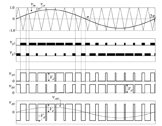
Fig:7 Waveform of Bipolar modulation scheme
Unipolar pwm inverter
The unipolar modulation normally requires two sinusoidal modulating waves’ vm and -vm which are of same magnitude and frequency but 1800 out of phase. The two modulating waves are compared with a common triangular carrier wave vcr generating two gating signals vg1 and vg3 for the upper two switches S1 and S3.
It is observed that the upper two devices do not switch simultaneously, which is distinguished from the bipolar PWM where all the four devices are switched at the same time. The inverter output voltage switches between either between zero and +Vd during positive half cycle or between zero and –Vd during negative half cycle of the fundamental frequency thus this scheme is called unipolar modulation. The unipolar switched inverter offers reduced switching losses and generates less EMI. On efficiency grounds, it appears that the unipolar switched inverter has an advantage.
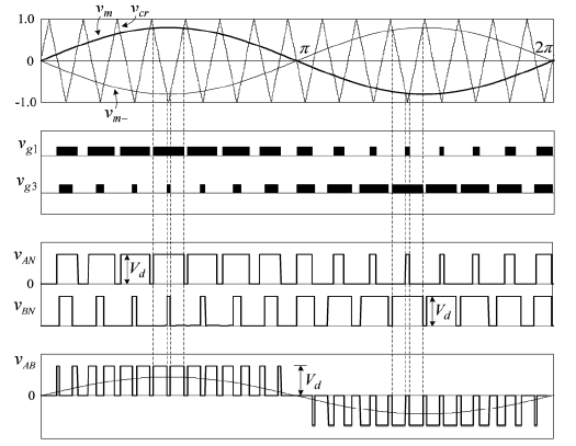
Fig:8 waveform of Unipolar modulation scheme
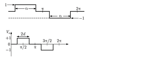
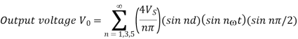
Q20) Explain any two harmonic elimination techniques for voltage source inverters?
A20) The high frequency harmonics if present in the output can be removed by using low-size filters. But to remove the lower order harmonics the size of filter increases. So, we require some other means to remove the lower order harmonics. The methods which can be implemented are explained below.
Harmonic Reduction by PWM
The method is already discussed above where there are several pulses per half cycle. Consider the waveform shown in figure below. Which is symmetrical about π as well as π/2.
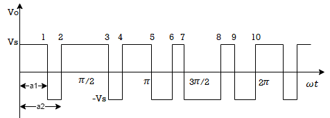
Fig 9 Harmonic reduction by PWM
The equation for this voltage will be
The third and fifth harmonics are eliminated
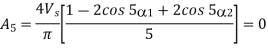
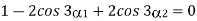
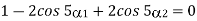
The above two equations can be solved in order to calculate α1, α2 under the condition that 0< α1<900 and α1< α2<900
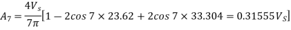

The amplitude of the fundamental component for these values of α1and α2 are
The amplitude of fundamental component of unmodulated output voltage wave is
The amplitude of the fundamental voltage is 0.8391 times the amplitude of fundamental components of unmodulated voltage wave.
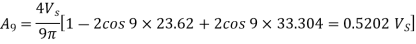
Harmonic Reduction by Transformer connections
The output voltage of the two or more inverters can be combined by means of transformers to get a net output voltage with reduced harmonic content. The necessary condition for this method is that the output voltage waveform from the inverter must be similar but phase shifted from each other. The output voltage v01 and v02 from inverter 1 and 2 respectively is shown below. The resultant v0 is obtained by adding vertical ordinates of v01 and v02.
The amplitude of V0 is 2Vs from interval π/3 to π and 4π/3 to 2π and so on.
Fig 10(a) Harmonic reduction by transformer connections (b) Elimination of harmonics
The Fourier Series for above waveform will be given as
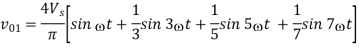

The voltage v0 is
V0 = v01+v02
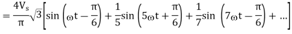
From above equation we can say that V01 leads 600 by V02 shown in figure below. The resultant of V01 and V02 should be √3 times V01 at the same time. For third harmonics V02 lags V01 by 1800 therefore the resultant is zero.
Fig 11 Phasor Diagram
For fifth harmonic V02 lags V01 by 3000 its resultant is √3 times V01or V02 and it leads V01 by 300. The resultant of fifth harmonic must be associated with √3 sin(ωt+π/6). In same manner the resultant of seventh harmonic is associated with √3 sin(ωt-π/6). The fundamental component of v0 is

When there is no phase shift between the output of two inverters then the amplitude of fundamental voltage is 8Vs/π. The disadvantage of this method is we need a greater number of inverters and transformers for similar ratings.


