Unit - 5
Single Phase DC-AC converter
Q1) (a) A single-phase full bridge inverter is connected to an RL load. For a dc source voltage of  and output frequency f=1/T, obtain expressions for load current as a function of time for the first two half cycles of the output voltage.
(b) Derive also the expressions for steady-state current for the first two half cycles.
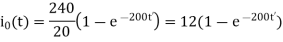
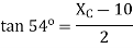
(c) For R=20  and L=0.1H, obtain current expressions for parts (a) and (b) in case source voltage is 240 V dc and frequency of output voltage is 50 Hz.
A1)
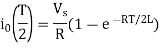
(a) For the first half cycle, for 0<t<T/2, the voltage equation for RL load is
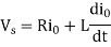
Its Laplace transform, with zero initial conditions is
Its time solution is,
 0<t<T/2
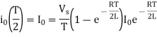
This is the expression of current as a function of time for the first half cycle from the instant of switching in with 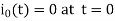
At  , current
  becomes the initial value of second half cycle.
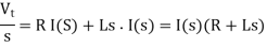
For second half cycle, time limit is from T/2 to T or 0<t’ <T/2 where t’=t-T/2. The voltage equation for RL load during second half cycle is
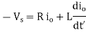
It Laplace transform with initial current  given by
Its time solution is 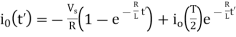
0 < t’ <T/2. The transient solution for load current for first and second half cycle respectively.
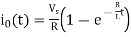
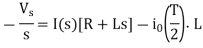
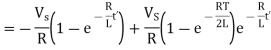
(b) Under steady-state conditions at t=0,  , under this condition Laplace transform
Its time solution is
At t=T/2 
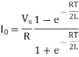
Substituting this value of 
The steady-state solution during the first half cycle i.e. for 0<t<T/2
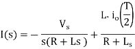
For second half cycle at t=T/2  , Under this initial condition,
Laplace transform0
The steady state solution during the second half cycle, ie for 0<t’<T/2 where t’=t-T/2
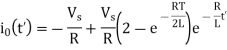
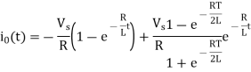
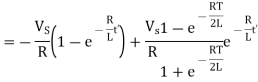
(c) Here 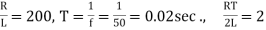
 during the first half cycle from
Expression for transient current for second half cycle,
Steady-state current for the first half cycle, ie for 0<t<T/2 is

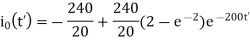
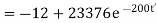
For the second half cycle, steady state current

 for 0<t’<T/2
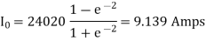
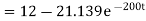
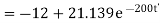
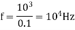
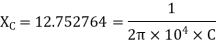
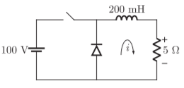
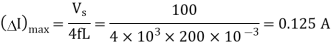
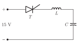
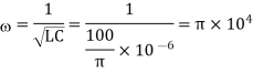
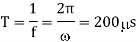
Q2) A single phase bridge inverter delivers power to a series connected RLC load with R=2 and L=10
 The periodic time T=0.1 msec. What value of C should the load have in order to obtain load commutation for the SCRs. The thyristor turn-off time is 10sec. The circuit turn off time as 1.5
 assume that load current contains only fundamental component.
A2)
The value of C should be such that RLC load is underdamped. Moreover, when load voltage passes through zero, the load current must pass through zero, the load current must pass through zero before the voltage wave, i.e. The load current must lead the load voltage by an angle θ as shown if fig 8.6. Recall the phasor diagram for RLC series circuit. From this phasor diagram
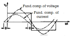
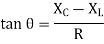
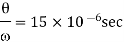
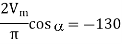
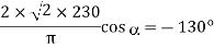
Here  as the current is leading the voltage. Now (θ/) must be at least equal to circuit turn-off time i.e. 1.5×10=15sec


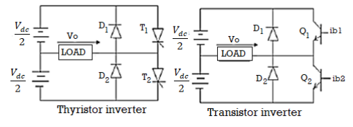
Q3) The single-phase half-bridge transistor inverter shown in Fig. Below has a resistive load of R = 3Ω and the d.c. Input voltage Vdc = 60 V. Determine:
(a) The rms value of the output voltage.
(b) The rms value of the load voltage at the fundamental frequency.
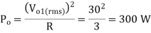
(c) The output power.
(d) The average and peak current of each transistor.
(e) The peak reverse blocking voltage VBR of each transistor.
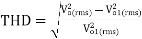
(f) The total harmonic distortion factor.
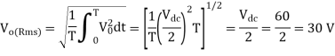
A3)
(a) The rms value of the output voltage is
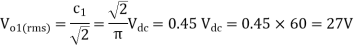
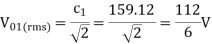
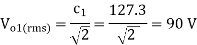
(b) The rms value of the load voltage at the fundamental frequency is
(c) The output powr is
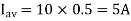
(d) The average and peak current of each transistor are
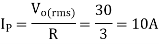
Because each transistor conducts for a 50% duty cycle, the average curret of each transistor is
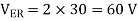
(e) The peak reverse blocking voltage  of each transistor is
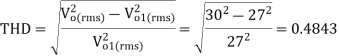
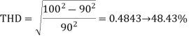
(f) The total harmonic distortion factor is
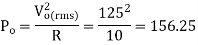
Q4) For the single-phase MOSFET bridge inverter circuit shown below, the source Vdc =125 V, load resistance R =10 Ω and output voltage frequency fo = 50 Hz.
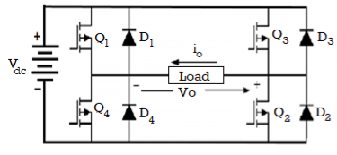
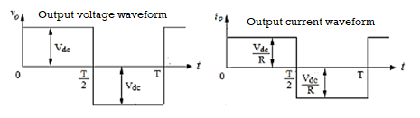
a) Draw the output voltage and load current waveforms.
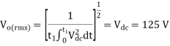
(b) Derive the rms value of the output voltage waveform and hence calculate the output power Po in terms of the output voltage.
(c) Analyse the amplitude of the Fourier series terms of the output voltage waveform by considering up to the 7th order harmonic. Determine the value of the rms output voltage in terms of harmonics rms values.
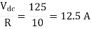
(d) Calculate the average and peak currents of each transistor.
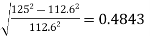
(e) Estimate the total harmonic distortion factor THD of the circuit.
A4)
(a)
(b) The rms value of the output voltage is
(c) The Fourier series of the output voltage is
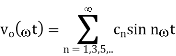
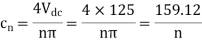
The amplitude  of the nth harmonic is:


Hence the output voltage fourier representation is,

In terms of harmonics
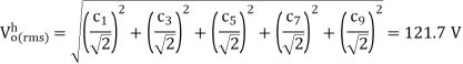
This value is less than  since we calculate up to 7th order harmonies only.
(d) Since the duty cycle of each transistor is 0.5, the current waveform is as shown below
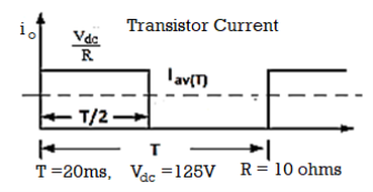
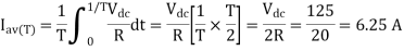
Peak current
(e)the total harmonic distortion factor.
 =
=
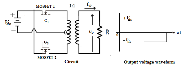
Q5) A single-phase MOSFET parallel inverter has a supply d.c. Voltage of 100V supplying a resistive load with R =10 Ω via a center-tap transformer with 1:1 ratio. The output frequency is 50 Hz.
(a) Draw the circuit diagram and the output voltage waveform of the inverter.
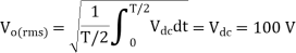
(b) Determine the rms value of the output voltage waveform.
(c) Determine the amplitude of the Fourier series terms for the square output voltage waveform up to 9th order harmonics.
(d) Calculate the rms value of the output voltage in terms of harmonic components that obtained in (b).
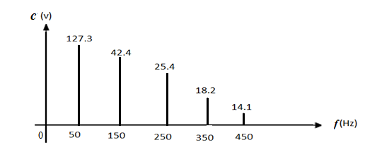
(e) Determine the power absorbed by the load consider up to 9th order harmonic.
(f) Draw the frequency spectra of the output voltage waveform.
(g) Calculate the total harmonic distortion factor THD.
A5)
(a) The circuit diagram and the output voltage waveform of the inverter
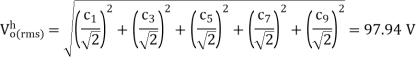
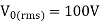
(b) The rms value of the output voltage is
(c) the Fourier series of the output voltage is
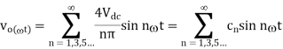
The amplitude cn of the n th order harmonic is:
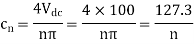


Hence the output voltage Fourier representation is,

(d) In terms of the harmonics, the rms value of the output voltage is
(e) To calculate the power, we most calculate the rms value of the current for each harmonic the amplitude of the nth harmonic current

Where  =R
=R
 |  |  |  |  |  |
1 | 50 | 127.3 | 10 | 12.73 | 810 |
3 | 150 | 42.4 | 10 | 4.24 | 89.8 |
5 | 250 | 25.5 | 10 | 2.55 | 32.5 |
7 | 350 | 18.2 | 10 | 1.82 | 16.5 |
9 | 450 | 14.1 | 10 | 1.41 | 9.99 |
The total power is 
(f) The frequency spectrum is given in Fig.
(g) The total harmonic distortion factor
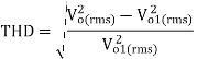
This is very high THD, the practical value of THD is about (3-10)% hence we need to use low-pass filter at the output to filter out most of the undesirable harmonic component and to produce nearly sinusoidal output waveform.
Q6) The three-phase inverter in Fig. Shown used to feed a Y-connected resistive load with R =15 Ω per-phase. The d.c. Input to the inverter Vdc = 300 V and the output frequency is 50 Hz. If the inverter is operating with 120˚ conduction mode, calculate: (a) The peak and rms value of the load current IL, (b) The output power, and the average and rms values of the current of each transistor.
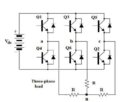
A6)
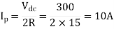
(a) For 120ᵒ conduction mode, at any time the load resistances of two phases are connected in series, hence, peak value of load current is
The rms value of the phase voltage is
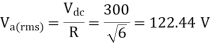
Hence the rms value of the load current is
(b) The load power is

(c) For 120ᵒ conduction mode, each transistor carries current for (1/3)rd of a cycle, hence the average transistor current is
The rms value of the thyristor current is
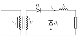
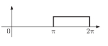
Q7) A half-controlled single-phase bridge rectifier is supplying an R-L load. It is operated at a firing angle a and the load current is continuous. The fraction of cycle that the freewheeling diode conducts is?
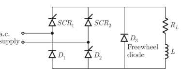
A7) The circuit of a single-phase half controlled bridge rectifier with RL load and free wheel diode is shown as below.
The voltage current wave forms are as shown below
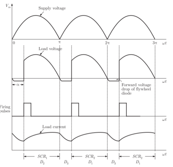
We note that, for continuous load current, the flywheel diode conducts from π to π+α in a cycle. Thus, fraction of cycle that freewheel diode conducts is α/π.
Thus fraction of cycle that freewheel diode conducts is a α/π.
Q8) A voltage commutated chopper circuit, operated at 500 Hz, is shown below. If the maximum value of load current is 10 A, then the maximum current through the main (M) and auxiliary (A) thyristors will be?
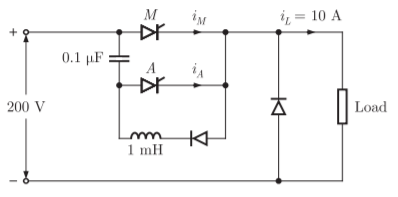
A8)
Maximum current through main thyristor
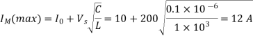
Maximum current through auxiliary thyristor
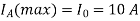
Q9) A single phase fully controlled converter bridge is used for electrical braking of a separately excited dc motor. The dc motor load is represented by an equivalent circuit as shown in the figure. Assume that the load inductance is sufficient to ensure continuous and ripple free load current. The firing angle of the bridge for a load current of I0 = 10 A will be?
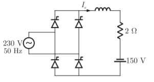
A9)
Here for continuous conduction mode by Kirchoff’s voltage law, average load current
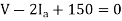

 So
So


Q10) A voltage commutation circuit is shown in figure. If the turn-off time of the SCR is 50 msec and a safety margin of 2 is considered, then what will be the approximate minimum value of capacitor required for proper commutation?
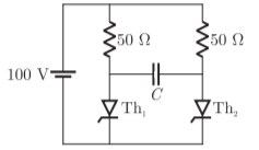
A10)
We know that 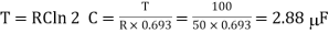
Q11) A solar cell of 350 V is feeding power to an ac supply of 440 V, 50 Hz through a 3-phase fully controlled bridge converter. A large inductance is connected in the dc circuit to maintain the dc current at 20 A. If the solar cell resistance is 0.5 W, then each thyristor will be reverse biased for a period of?
A11)
Let we have

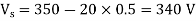

So each thyristor will reverse biased for 
Q12) The figure shows the voltage across a power semiconductor device and the current through the device during a switching transition. If the transition a turn ON transition or a turn OFF transition? What is the energy lost during the transition?
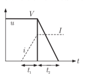
A12) In Ideal condition we take voltage across the device is zero. Average power loss during switching= (VI/2) (t1 + t2) (turn ON)
Q13) The given figure shows a step-down chopper switched at 1 kHz with a duty ratio D = 0.5. The peak-peak ripple in the load current is close to
A13)
Duty ratio 
Here 
Ripple 
Q14) Thyristor T in the figure below is initially off and is triggered with a single pulse of width 10  s. It is given that L = (100/π)
 H and C= (100/ π)
  F. Assuming latching and holding currents of the thyristor are both zero and the initial charge on C is zero, T conducts for?
A14)
Given 
 when the circuit is triggered by 10s pulse, the thyristor is short circuited and so, we consider
Therefore, the voltage stored across capacitor is

Where is angular frequency obtained as
As  oscillates betwee –ve and –ve half cycle so circuit is conductng for only half of cycle and thyristor is open after half cycle.
The conduction period 
Q15) A single-phase, 230 V, 50 Hz ac mains fed step down transformer (4:1) is supplying power to a half-wave uncontrolled ac-dc converter used for charging a battery (12 V dc) with the series current limiting resistor being 19.04 W. The charging current is?
A15)
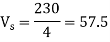
Here charging current=I

 radian


There is no power consumption in battery due to ac current, so average value of charging current
Q16) The minimum approximate volt-second rating of pulse transformer suitable for triggering the SCR should be: (volt-second rating is the maximum of product of the voltage and the width of the pulse that may applied?
A16)
We know that the pulse width required is equal to the time taken by  to rise upt
So 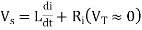
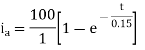


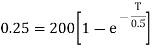
Width of pulse =187.6s
Magnitude of voltage=10V
 rating of P.T=10×187.6s=1867 V-s is approx to 2000 V-s
Q17) A single-phase half wave uncontrolled converter circuit is shown in figure. A 2-winding transformer is used at the input for isolation. Assuming the load current to be constant and V = Vm sin wt, the current waveform through diode D2 will be?
A17) In first half cycle D1 will conduct and D2 will not and at q = 0 there is zero voltage. So current wave form is as following
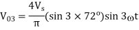
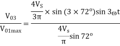
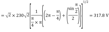
Q18) A single-phase inverter is operated in PWM mode generating a single-pulse of width 2d in the centre of each half cycle as shown in figure. It is found that the output voltage is free from 5th harmonic for pulse width 1440. What will be percentage of 3rd harmonic present in the output voltage (V03/V01max)?
A18)
In the PWM inverter
 output voltage of inverter
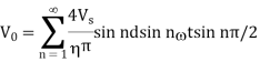
So the pulse width =2d =
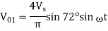
Q19) The triac circuit shown in figure controls the ac output power to the resistive load. The peak power dissipation in the load is?
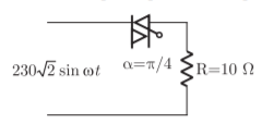
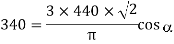
A19)
Output dc voltage across load is given as following
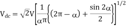
Losses 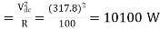
Q20) Explain the voltage control techniques for 3-phase voltage source inverter?
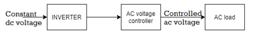
A20) When there are AC loads it requires the voltage to be maintained or controlled at the input terminals. When inverters are used for such loads, we ned the output voltage to be in control. Because the requirements of AC loads can be fulfilled.
(a) External control of AC output voltage:
This can be done by AC voltage control in which an ac voltage controller is connected in between the output terminals of inverter and the load. The below figure shows the connections. The voltage input to the ac load is regulated through the firing angle control of ac voltage controller. But there are harmonics in the output when the output voltage from the ac voltage controller is at low level.
The other method is series inverter method which consists of two or more inverters which are connected in series. Figure below shows that the output voltage of two inverters is summed with the help of transformer. The secondaries of the transformer is connected in series having input as the inverters output. The resultant voltage from the phasor is then
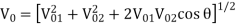
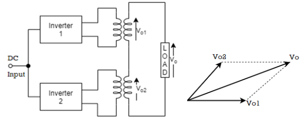
Fig 2 Series Inverter Control of two inverters
The essential condition for this is V01, V02 should be equal.
When  =0
=0
V0= V01+ V02
When  =π
=π
V0 = 0 only when V01= V02
As inverters are connected in series this method is also called as multiple converter control.
(b) External control of dc Input Voltage
AC voltage source is present here. The input to the converter which is dc voltage is controlled through the fully controlled rectifier (a). Alternate method is to use an uncontrolled rectifier and a chopper (b). The other way is to use an ac voltage controller and an uncontrolled rectifier (c). If the available volage is dc then dc voltage input to the inverter is controlled by means of a chopper as shown in figure below.
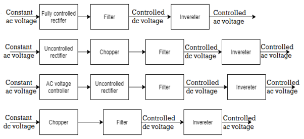
Fig 3 External control of dc input voltage to inverter
The output voltage waveform and its harmonics are not affected as the output voltage of inverter is controlled through the adjustment of dc input to the inverter.
(c) Internal control of Inverter
By adjusting the voltage within the inverter, the output voltage can be adjusted. The is can be achieved by pulse width modulation control (PWM). In PWM method the inverter is fed with fixed dc input voltage and a controlled ac output voltage is obtained by adjusting the ON and OFF periods of the inverter.
No additional components are required to adjust the voltage. The lower harmonic orders are also eliminated. The higher order harmonics can be filtered easily. The main disadvantage of this method is that the SCR are expensive as they must possess low turn on and turn off times.


