Unit – 2
Transistor based Devices and DC-DC converter
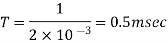
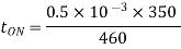
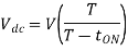
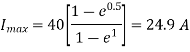
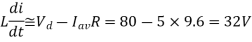
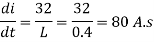
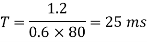
Q1) A Chopper circuit is operating on TRC at a frequency of 2 kHz on a 460 V supply. If the load voltage is 350 volts, calculate the conduction period of the thyristor in each cycle.
A1)

Chopping period 
Output voltage 
Conduction period of thyristor


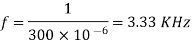
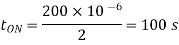
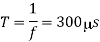
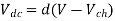
Q2) Input to the step up chopper is 200 V. The output required is 600 V. If the conducting time of thyristor is 200 µsec. Compute – Chopping frequency, – If the pulse width is halved for constant frequency of operation, find the new output voltage.
A2)

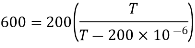
Solving for T
T=200s
Chopping frequency 
Pulse width is halved
Frequency is constant 
Output voltage 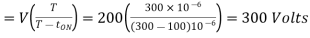
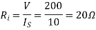
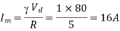
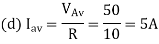
Q3) A dc chopper has a resistive load of 20Ω and input voltage VS = 220V. When chopper is ON, its voltage drop is 1.5 volts and chopping frequency is 10 kHz. If the duty cycle is 80%, determine the average output voltage and the chopper on time.
A3) 

 Voltage drops across chopper =1.5 volts
Average output voltage

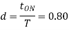
 Voltage drops across chopper=1.5 volts
Average Output voltage

Chopper ON time 
Chopping period, 
Chopper ON time


Q4) In a dc chopper, the average load current is 30 Amps, chopping frequency is 250 Hz, supply voltage is 110 volts. Calculate the ON and OFF periods of the chopper if the load resistance is 2 ohms.
A4)


 and
and 

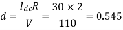
Chopper ON period

Chopper OFF period


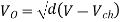
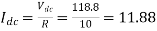
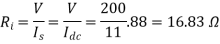
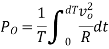
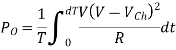
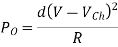
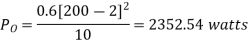
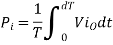
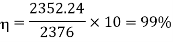
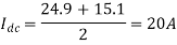
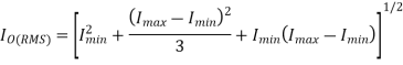
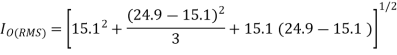
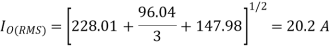
Q5) A dc chopper in figure has a resistive load of and input voltage of V = 200 V. When chopper is ON, its voltage drop is 2 V and the chopping frequency is 1 kHz. If the duty cycle is 60%, determine Average output voltage RMS value of output voltage Effective input resistance of chopper Chopper efficiency.
V=200V, R=10 , Chopper voltage drop,
  d=0.60, f=1 kHz
Average output voltage

RMS value of output voltage

Effective input resistance of chopper is

 Amps
Amps
Output Power:
Input Power:

Chopper efficiency

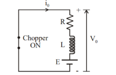
Q6) A chopper feeding on RL load is shown in figure, with V = 200 V, R = 5, L = 5 mH, f = 1 kHz, d = 0.5 and E = 0 V. Calculate – Maximum and minimum values of load current. – Average value of load current. – RMS load current. – Effective input resistance as seen by source. – RMS chopper current.
A6)
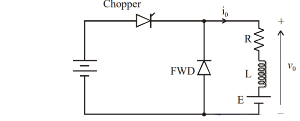
V=200V R=5
F=1kHz, d=0.5, E=0
Chopping period is
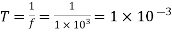 secs
secs
Maximum value of load current is given by
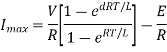
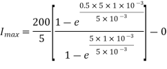
Minimum value of load current is given by
Average value of load current is

For linear variation of currents
RMS load current is given by
RMS chopper current is given by

Effective input resistance is

 Average source current
Therefore, effective input resistance is
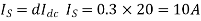
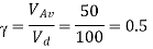
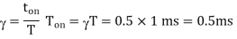
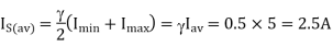
Q7) A transistor dc chopper circuit (Buck converter) is supplied with power form an ideal battery of 100 V. The load voltage waveform consists of rectangular pulses of duration 1 ms in an overall cycle time of 2.5 ms. Calculate, for resistive load of 10 Ω. (a) The duty cycle γ. (b) The average value of the output voltage Vo. (c) The rms value of the output voltage Vorms. (d) The ripple factor RF. (e) The output dc power.
A7)
(a) 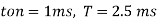
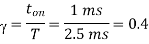
(b) 
(c)
(d) 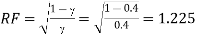
(e) 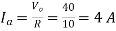

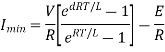
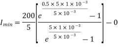
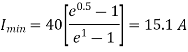
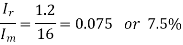
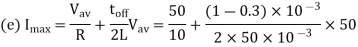
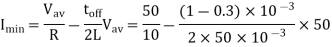
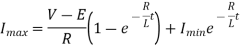
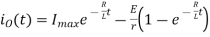
Q8) An 80 V battery supplies RL load through a DC chopper. The load has a freewheeling diode across it is composed of 0.4 H in series with 5Ω resistor. Load current, due to improper selection of frequency of chopping, varies widely between 9A and 10.2. (a) Find the average load voltage, current and the duty cycle of the chopper. (b) What is the operating frequency f? (c) Find the ripple current to maximum current ratio.
A8)
(a) The average load voltage and current are


(b) to find the operating (chopping) frequency
During the ON period

Assume  constant
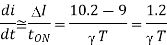
From eq (1)
But 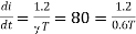
Hence 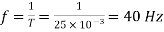
The maximum current  occurs at =1
Ripple current 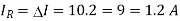
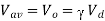
Q9) A DC Buck converter operates at frequency of 1 kHz from 100V DC source supplying a 10 Ω resistive load. The inductive component of the load is 50mH.For output average voltage of 50V volts, find: (a) The duty cycle (b) ton (c) The rms value of the output current (d) The average value of the output current (e) Imax and Imin (f) The input power (g) The peak-to-peak ripple current.
A9)
(a) 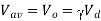
(b) 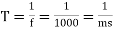


(g) 
Q10) Draw and explain the class B chopper with its operation?
A10) CLASS B CHOPPER
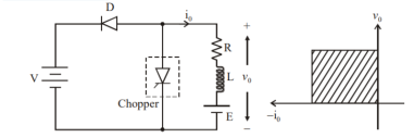
Figure 1 Class B chopper
Fig. Shows a Class B Chopper circuit. When chopper is ON, and E drives a current through L and R in a direction opposite to that shown in figure. During the ON period of the chopper, the inductance L stores energy.
When Chopper is OFF, diode D conducts, and part of the energy stored in inductor L is returned to the supply. Also, the current continues to flow from the load to source. Hence the average output voltage is positive and average output current is negative.
Therefore, Class B Chopper operates in second quadrant. In this chopper, power flows from load to source. Class B Chopper is used for regenerative braking of dc motor.
Figure (b) shows the output voltage and current waveforms of a Class B Chopper. The output current equations can be obtained as follows. During the interval diode ‘D’ conducts (chopper is off) voltage equation is given by
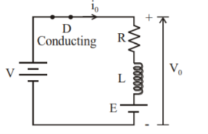
For the initial condition i.e., at. The solution of the above equation is obtained along similar lines as in step-down chopper with R-L load
Therefore 
At 

During the interval chopper is ON voltage equation is given by
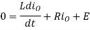
Redefining the time origin, at t=0, 
The solution for the stated initial condition is


Therefore 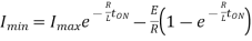
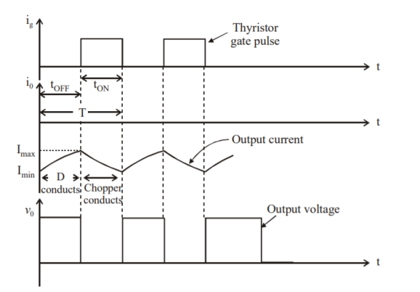
Figure 2. Class B Chopper Output Voltage and current waveform.
Q11) Explain the four quadrant operation of DC chopper?
A11) Class E chopper:
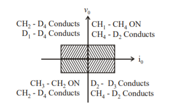
Four Quadrant Operation
Figure 3. Class E chopper
Figure shows a class E 4 quadrant chopper circuit. When they are triggered, output current flows in positive direction as shown in figure through and, with output voltage vo=V. This gives the first quadrant operation.
When both and are OFF, the energy stored in the inductor L drives through and in the same direction, but output voltage vo=-V. Therefore, the chopper operates in the fourth quadrant.
For fourth quadrant operation the direction of battery must be reversed. When Ch2 and Ch3 are triggered, the load current io flows in opposite direction and output voltage vo = -V. Since both io and vo are negative, the chopper operates in third quadrant.
When both CH2 and CH3 are OFF, the load current io continues to flow in the same direction through D1 and D4 and the output voltage vo=V. Therefore, the chopper operates in second quadrant as vo is positive but io is negative. Figure shows the devices which are operative in different quadrants.
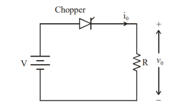
Q12) Explain the principle and working of DC-DC converter?
A12) Principle of operation of chopper
Chopper circuits are known as DC to DC converters. Choppers are used to step up and step down the DC power. They change the fixed DC power to variable DC power. Using these, DC power supplied to the devices can be adjusted to the required amount.
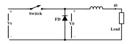
Figure 4. Chopper circuit
The principle of operation of chopper can be understood from the circuit diagram below.
The circuit consists of semiconductor diode, resistor, and load. For all type of chopper circuit, the output voltage value is controlled by periodic closing and opening of the switches used in the circuit.
The chopper can be viewed as an ON/OFF switch that can rapidly connect or disconnect the source to load connection. Continuous DC is given as source to the chopper as Vs and chopped DC is obtained across the load as V0.
Output Voltage and Current Waveforms
The output voltage and current waveforms of a chopper circuit are shown in figure. From the voltage waveform, it seen that during the period of TON the load voltage V0 is equal to the source voltage Vs.
But when the interval TOFF occurs, the DC voltage step downs to zero, thus making the load short-circuited.
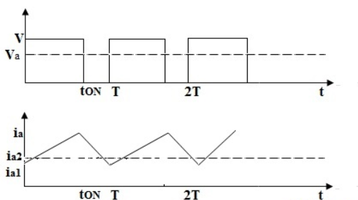
Figure 5. Output Waveform
- In the current waveform, during the interval TON the load current rises to the maximum value. During the interval TOFF, the load current decays.
- In TOFF condition the chopper is off so the load voltage becomes zero.
- But load current flows through the diode FD, making the load short-circuited.
- Thus, the chopped DC voltage is produced at the load.
- The current waveform is continuous which rises during TON state and decays during TOFF state.
Q13) What are static and dynamic characteristics of MOSFET?
A13) Static characteristics:
Drain-source on-state resistance (RDS(ON))
The resistance across drain and source when the MOSFET is in the "on" state.
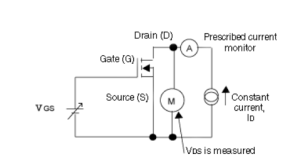
Figure 6. Static Characteristics
The specified constant drain current, ID, is applied until VGS reaches the specified voltage. At this point, drain-source voltage is measured. On-state resistance is calculated by dividing it by the value of drain current, ID.
Measurement of forward transfer admittance
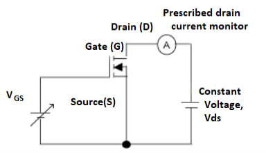
Gate-source voltage, VGS, is increased until drain current, ID, reaches the specified value. Then, VGS is changed only slightly, and the resulting change in drain current, ID, is measured.
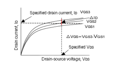
Figure 7 Change in VGS w.r.t ID
Dynamic Characteristics
Since power MOSFETs are majority-carrier devices, they are faster and capable of switching at higher frequencies than bipolar transistors.
Switching time measurement circuit and input / output waveform are shown below.
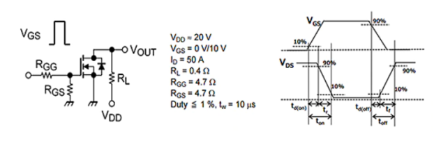
Figure 8. Dynamic Characteristics
td (on): Turn-on delay time
The time from when the gate-source voltage rises above 10% of VGS until the drain-source voltage reaches 90% of VDS
tr: Rise time
The time taken for the drain-source voltage to fall from 90% to 10% of VDS
ton: Turn-on time
The turn-on time is equal to td (on)+ tr.
td (off): Turn-off delay time
The time from when the gate-source voltage drops below 90% of VGS until the drain-source voltage reaches 10% of VDS
tf: Fall time
The time taken for the drain-source voltage to rise from 10% to 90% of VDS
toff: Turn-off time
The turn-off time is equal to td(off)+ tf.
Q14) Compare MOSFET and IGBT?
A14)
Features | MOSFET | IGBT |
Drive Method | Voltage | Voltage |
Drive Circuit | Simple | Simple |
Input Impedance | High | High |
Drive Power | Low | Low |
Switching Speed | Fast(ns) | Middle |
Operating Frequency | Fast (less than 1MHz) | Middle |
S. O. A | Wide | Wide |
Saturation Voltage | High | Low |
Q15) Draw and explain the switching characteristics of IGBT?
A15) The IGBT is a Voltage controlled device, hence it only requires a small voltage to the gate to stay in the conduction state. And since these are unidirectional devices, they can only switch current in the forward direction which is from collector to emitter.
A typical switching circuit of IGBT is shown below, the gate volt VG is applied to the gate pin to switch a motor (M) from a supply voltage V+. The resistor Rs is roughly used to limit the current through the motor.
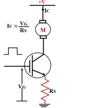
Figure 9. Switching characteristics
The input characteristics of IGBT can be understood from the graph below.
Initially, when no voltage is applied to the gate pin the IGBT is in turn off condition and no current flows through the collector pin. When the voltage applied to the gate pin exceeds the threshold voltage, the IGBT starts conducting and the collector current IG starts to flow between the collector and emitter terminals. The collector current increases with respect to the gate voltage as shown in the graph below.
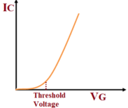
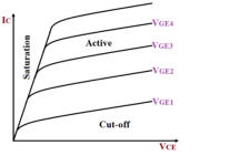
Figure 10. Output characteristics
- The output characteristics of IGBT have three stages,
- Initially, when the Gate Voltage VGE is zero the device is in the off state, this is called the cut-off region.
- When VGE is increased and if it is less than the threshold voltage then there will be a small leakage current flowing through the device, but the device will still be in the cut-off region.
- When the VGE is increased beyond the threshold voltage the device goes into the active region and the current starts flowing through the device. The flow of current will increase with an increase in the voltage VGE as shown in the graph above.
Q16) Compare non-punch through and punch through IGBT?
A16)
Punch through IGBT (PT-IGBT) | Non-Punch Through- IGBT (NPT- IGBT) |
These are less rugged in short-circuit failure mode and has less thermal stability | These are more rugged in short circuit failure mode and has more thermal stability. |
The collector is a heavily doped P+layer | The collector is a lightly doped P+layer |
It has a small positive temperature coefficient of ON- State voltage, hence parallel operation requires great care and attention. | The temperature coefficient of ON-state voltage is strongly positive, hence the parallel operation is easy. |
The turn off loss is more temperature-sensitive, hence it increases significantly at a higher temperature. | The turn off a loss is less temperature-sensitive, so, it will remain unchanged with temperature.
|
Q17) Explain construction and working of IGBT?
A17) IGBT (Insulated Gate Bipolar Transistor)
It is a three-terminal semiconductor switching device that can be used for fast switching with high efficiency used in many types of electronic devices.
These devices are used in amplifiers for switching/processing complex wave patters with pulse width modulation (PWM).
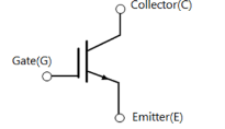
Figure 11. IGBT symbol
IGBT is constructed with equivalent circuit that consists of two transistors and MOSFET.IGBT combines the low saturation voltage of a transistor with the high input impedance and switching speed of a MOSFET. The outcome obtained from this combination delivers the output switching and conduction characteristics of a bipolar transistor, but the voltage is controlled like a MOSFET.
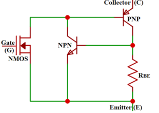
Figure 12. Internal structure
- IGBT has three terminals attached to three different metal layers, the metal layer of the gate terminal is insulated from the semiconductors by a layer of silicon dioxide (SIO2).
- IGBT is constructed with 4 layers of semiconductor sandwiched together. The layer closer to the collector is the p+ substrate layer above that is the n- layer, another p layer is kept closer to the emitter and inside the p layer, we have the n+ layers.
- The junction between the p+ layer and n- layer is called the junction J2 and the junction between the n- layer and the p layer is called the junction J1.
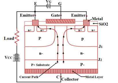
Figure 13. Construction of IGBT
Working:
- Consider a voltage source VG connected positively to the Gate terminal with respect to the Emitter. Consider other voltage source VCC connected across The Emitter and the Collector, where Collector is kept positive with respect to the Emitter.
- Due to the voltage source VCC the junction J1 will be forward-biased whereas the junction J2 will be reverse biased. Since J2 is in reverse bias there will not be any current flow inside the IGBT (from collector to emitter).
- Initially, when no voltage applied to the Gate terminal, at this stage the IGBT will be in non-conductive state. As we increase the applied gate voltage, due to the capacitance effect on the SiO2 layer the negative ions will get accumulated on the upper side of the layer and the positive ions will get accumulated on the lower side of the SiO2 layer.
- This will cause the insertion of negative charge carriers in the p region,
- The higher the applied voltage VG greater the insertion of negatively charged carriers. This will lead to a formation of the channel between the J2 junction which allows the flow of current from collector to emitter.
- The flow of current is represented as the current path in the picture, where the applied Gate voltage VG increases the amount of current flow therefore the collector to the emitter also increases.
Q18) What are MOSFETs. Explain depletion and enhancement mode MOSFET?
A18) The MOSFET is a four-terminal device with source(S), gate (G), drain (D) and body (B) terminals. The body of the MOSFET is frequently connected to the source terminal making it a three- terminal device like field effect transistor.
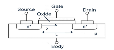
Figure 14. MOSFET
The MOSFET works by varying the width of a channel along which charge carriers flow (electrons or holes). The charge carriers enter the channel at source and exit via the drain.
The width of the channel is controlled by the voltage on an electrode is called gate which is located between source and drain. It is insulated from the channel near an extremely thin layer of metal oxide.
The MOS capacity present in the device is primary.
The MOSFET can function in two ways
- Depletion Mode
- Enhancement Mode
Depletion Mode:
Figure 15. Depletion mode
When there is no voltage on the gate, the channel displays maximum conductance. As the voltage on the gate is either positive or negative, the channel conductivity decreases.
Enhancement Mode
When there is no voltage on the gate the device does not conduct. More is the voltage on the gate, the better the device can conduct.
Figure 16. Enhancement mode
Working:
- The working of MOSFET depends upon the MOS capacitor. The MOS capacitor forms main part of MOSFET. The semiconductor surface at the below oxide layer is located between the source and drain terminal
- It can be inverted from p-type to n-type by applying a positive or negative gate voltage respectively. When we apply the positive gate voltage the holes present under the oxide layer with a repulsive force and holes are pushed downward with the substrate.
- The depletion region populated by the bound negative charges which are associated with the acceptor atoms. The electrons reach channel is formed.
- The positive voltage also attracts electrons from the n+ source and drain regions into the channel.
- Now, if a voltage is applied between the drain and source, the current flows freely between the source and drain and the gate voltage controls the electrons in the channel. Instead of positive voltage if we apply negative voltage, a hole channel will be formed under the oxide layer.
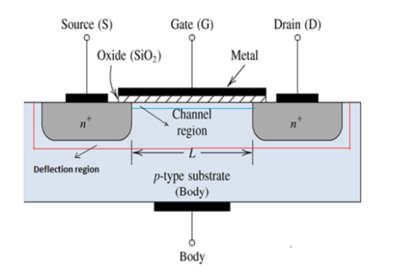
Figure 17. MOSFET construction


