Unit 06
Nanotechnology
Q1) What is nanotechnology and what are nano materials. Do they exist in nature?
A1) Nanotechnology comprises nanoscale research, engineering and technology, that is roughly 1 to 100 nanometers. A nanometer is a milliard of a meter. A sheet of paper is about 100000 nanometers thick, for comparison. Nano scale substance can behave differently from the same bulk materials. For example the melting point of substance, strength, chemical, color and reactivity and researchers seeking to understand the nature of nano scale properties may call their work nanoscience, those focusing on the properties being used successfully may call their work nano engineering. Nanotechnology covers nanoscale research, engineering and technology and includes the visualization, calculation, simulation and manipulation of nanoscale matter.
The word “nanomaterials” refers to the nano-scale materials, or materials containing nano scale structure inside or on their surfaces. These can be involves nanometer scale engineered objects such as nanoparticles, naotubes and nano films as well as naturally occurring nano particles such as volcanic ash, sea spray and smoke.
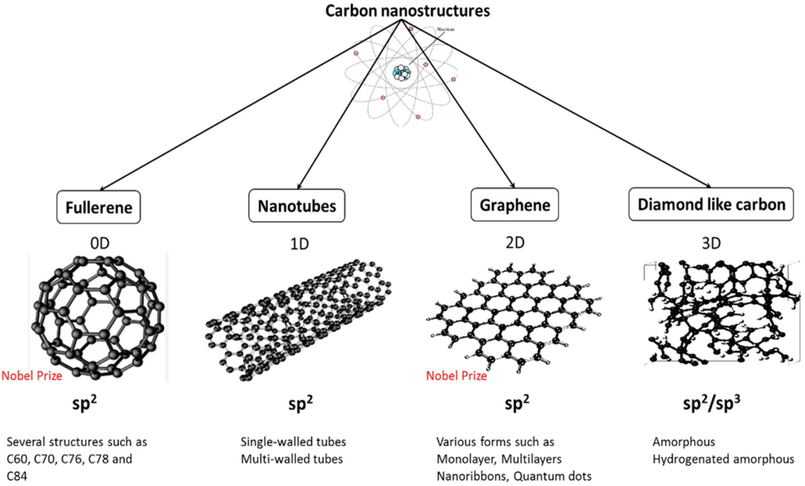
Q2) Explain carbon nano structures?
A2) In the structure of carbon nanostructures involves different type of low dimensional carbon allotropes including the carbon black, fullerene, carbon fiber, graphene and carbon nanotubes (CNTs). Graphene and CNTs have unique properties. CNTs have great mechanic properties and these are the strongest one.
Concepts
1970- Osawa, a molecule is made up from SP2 hybridized carbons have a soccer type structure.
1973- Gal’pern and Bochvar, provide C20 and C60 structures and their properties.
1985- Kroto, this is a concept of the experiment with the vaporized carbon.
Fullerene
This is the allotrope of carbon whose molecule keeps of the carbon atoms which is connected through double and single bonds, therefore to from a partially closed mesh with the fused rings of 5 to 7 atoms. And the molecule may be ellipsoid, hollow sphere, tube or many other sizes and shapes.
The explained structure for the C, a “truncated icosahedrons”, is extracted from an icosahedrons through truncating or “shipping off” every of the 12 vertices. Every vertex is replaced through 5 membered ring, pentagon. This snipping procedure also changes each of 20 former triangular face into the 6 mentioned rings hexagons.
Nano-tubes
There are many carbon nanotubes applications and properties that take complete benefits of the CNTs features like ratio, thermal conductivity, electrical mechanical strength. The kinds of the carbon nanotubes are crucial mentioned to as single walled carbon Nanotubes and multi walled carbon Nanotubes.
Q3) Explain various concepts of the energy bands in nanotechnology.
A3) To better understanding many of properties of the nanostructure materials, a fundamental knowledge of band diagram is needed, together with knowledge of this concepts as the bandgap energy, holes and exictons and direct and indirect bandgaps. A band diagram represents energy of a permitted state of the charge carrying particle in a specific material as a momentum functions or, due to wave-particle duality, as the function of wave vector ~ k. The wave magnitude vector is wave number indicated by the k. In a band diagram, the permitted energy states are assembelled into the bands, the conduction band and valence band being more important bands for properties description of the many materials. As wave vector is the 3D quantity, band diagram must be 4D plots. But, very generally only 2D and 3D plots for the significant ranges of wave vector direction is drawn, moreover, symmetries generally permit 3D plots to be made as the 2D plots.
Below figure presents tough 1D band diagrams for the direct/indirect bandgap semiconductors, the wave direction vector being determined, however not its magnitude. The 2 basic features which play an essential role in behavior of nay material can be obtained from a band diagram-
Bandgap energy Eg
Whether bandgap is direct/indirect.
The bandgap is energy range where in no state is allowed for the charge carriers to engaged. As bandgap energy is explained as energy difference between lowest point of conduction band and highest point of valence band, Eg is consider as the vertical distance between two bands in band diagram. Crucial values of bandgap energy at the room temperature are-
Eg (Si) =1.11 eV
Eg(Ge) =0.66 eV
Eg (GaAs) = 1.43 eV
Eg (CdS) =2.42 eV
Eg (InP) = 1.27 eV
The bandgaps traversal through charge carriers includes the net exchange of energy between charge carriers on one hand and photons or phonons on the other. Energy photons ~ω are light quanta. Phonons of energy ~ω are also the quantum particles, being explained as the excitation quanta of crystalline lattice vibration angular modes frequency ω. The idea of a phonon arises from a quantum mechanical lattice treatment vibration in the solid, supposing that a lattice vibration mode is analogous to an easy harmonic oscillation. Phonons are play an essential role in behavior of the solids through influencing their electrical, thermal and electrical properties by interactions with the photons, neutrons and electrons etc.
Band gap can be directed or indirect. In direct band gap material maximum energy of valence band and minimum of conduction band occur at similar value of momentum, as explained in figure (a). Either the photons are supply essential energy for the particle to climb to the conduction band from valence band or the photons are emitted during particle transition from the conduction band of valence band. Any phonons are participating in transitions from valence or conduction band to valence or conduction band. Most of the III-V compound semiconductor, like as GaAs are direct bandgap semiconductor and broadly utilized for optoelectronic applications. In an indirect band-gap semiconductor is one in that maximum energy of valence band and lowest energy of conduction band occur at the various values of momentum, as shown in figure (b). Since the momentum (when addition to energy) should be conserved in any of the interbond transition, phonons require to participate in these transition, developing these transitions less probably (or less efficient) in the indirect gap semiconductors. Germanium and silicon is examples of indirect gap semiconductors, with the limited use of practical in the opto electronic.
By charge carriers energy bands are famous that is holes and electrons. Holes are the virtual entities which can be thought as the electron vacancies. The hole charge is opposite in the sign however equal in the magnitude to which of an electron. The effective mass of the hole is somewhat variant from which of an electron, their respective impact masses being relied on the curvatures of conduction and valence bands. An excitation is quasi- particle containing an electron and a hole bound to each other. As an energy excitation’s is somewhat below the band gap energy, slightly transitions is lower energy than Eg become potential. Excitations can move by a transport and material energy, though they do not transport charge as because they electrically neutral. Tough binding energies of the excitations are Eex (Si)= 14.7 meV
Eex (Ge) 4.15 meV
Eex (GaAs) =4.2 meV
Eex (CdS) = 29.0 meV,
Eex (InP) = 4.0 meV
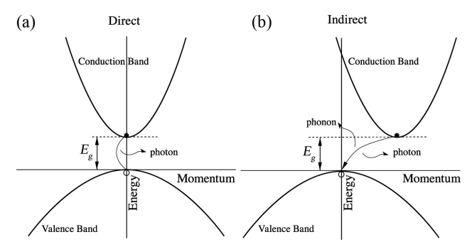
One dimensional band diagram having (a) direct and (b) indirect bandgaps.
These 2D plots are named 1D band diagram because direction of wave vector (or momnetum) has been determined, however its magnitude is permitted to differ.
Conduction mechanism in Nano-structures
It is based on the naval surface warfare centre, Dahelgren division, has been interface research problems involved with the liquid dielectrics for 3 decades-
Water electrolytes modeling efforts have been progressed by traditional mechanism to include the charge injection. Currently work has been extended in the field of nano-technology and outcome in the measurement of the conductance by the water electrolyte wetted nano structured. The nano structures utilized were samples which were produced through the naval research laboratory and donated to NSWC. The validation key to the improved conduction double layer model is like reasonable values to the double layer improved and thickness mobility can caount to the experimental observations. Those parameter is fitted by a trial and error procedure bounded through physical expectations to the water electrolytes. There are some expected boundaries involved-
Improved mobility limit equal to the ratio of dielectric constant in bulk which in the double layer. In practical this consider less than a factor of the 78 at the room temperature, however since dielectric constant of double layer is mostly calculated between 2 and 6, and the upper limit would better as above 40.
Double layer thickness limit to some of the multiple of debye length in the water electrolyte, that is 3.033nm at the room temperature in the 0.01M NaCl.
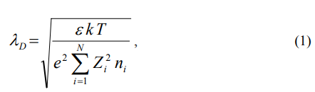
With the ΛD = Debye length
ε = water dielectric constant, at room temperature of the 25
k = Boltzmann constant = 1.380658 x 10⁻²³ J/K
T = temperature in K, room temperature = 298.15K
e =electronic charge, 1.60217733 x 10⁻¹⁹ coulombs
Zi = ith conducting ion valence in the electrolyte water
Ni= ith conducting ion number density in the electrolyte water, this is in the terms of the ions number per cubic meter.
Q4) Define BN nanotubes.
A4) BNNTs (boron nitride nanotubes) are a boron nitride polymorph. These were predicted in the year 1994 and discovered in the year 1995. They are similar with the carbon nnaotubes in structure, that are cylinders with the sub-micrometer diameters and lengths of the micrometer, except which carbon atoms are alternately reliefed through boron and nitrogen atoms. But, the properties of the BN nanotubes are too different, whereas carbon nanotubes can be semiconducting or metallic relying on rolling direction and radius, a BN nanotubes are electrical insulator with the band gap of ~ 5.5 eV, fundamentally independent of tube morphology and chirality.
Synthesis and production
A well developed techniques of the carbon nanotube growth, like arc-discharge, chemical vapor deposition and laser ablation are utilized for the mass production of BN nanotube at a tens of grams scale. These can also be developed through ball milling of the amorphous boron, mixed with the catalyst (iron powder), under the NH3 atmosphere.
Properties and potential applications
Properties of the BN nanotubes like electrical and field emission can be tuned through doping with the gold atoms by gold sputtering on nanotubes.
BNNs are utilized in the cancer treatments due to their high stiffness and best chemical stability.
Q5) Why are nano materials are used in cosmetics?
A5) In the new cosmetic regulation (EC) no 1223/2009 which comes into force in the EU on the 11 july 2013, nano materials were taken into the account for the first time. What has been and will continue to the case for UV philters up to now is that the EU commission will decide on their inclusion in the positive list of UV philters approved in the cosmetics after a risk assessment. The scientific committee for consumer safety (SCCS, formerly SCC, SCCNFP, SCCP), which advise the EU commission, will make this at european level. The notes of guidance form the basis for the risk assessment. For example, nanoparticles made of titanium dioxide and zinc oxide are to be used in sun creams as UV philters to protect the skin against UV radiation. The purpose of nanotechnology manufacture materials in toothpaste is to promote the natural saliva repair mechanism for the tooth. The purpose of nanocapsules in skincare products is to ensure the protection and transport of active ingredients and to improve the effect of care. Research is being carried out with the help of nanomaterials to improve the physical properties of finished cosmetics.
Q6) Is it possible to design the hazard with something like nanosilver while keeping the “benefits”?
A6) This is a challenging one. Being able to do this will be good and there could be some possibilities here. Silver destroys microbes primarily by releasing silver ions which are harmful to many microbes. Silver nano particles are effective in releasing ions faster than the same amount of larger particles and can be applied to a broad variety of items. There is also some evidence that the nano particles may be toxic to microbes themselves. The big issue here is you need the ions to be successful and if they release the silver ions into the atmosphere they might do more than just destroy the microbes they want them to. But if there was a way to restrict the release rate and just ensure the microbes that they want to get rid of coming into contact with the silver ions, it might be possible to minimize potential risks while increasing benefits. Some of the more sophisticated applications of silver as an antimicrobial tend to be taking that approach . The thing they really don’t want to do here is unthinkingly release silver nano particles into the atmosphere, where they will continue releasing ions and potentially causing harm.
Q7) Are there appropriate respirator philters to protect against inhalation given the nano-size of the particles?
A7) Yes, there are some unanswered questions here but in general, respirator philters are better than larger particles to remove particles of nano meter size from the air. It sounds counter intuitive but Brownian motion is the key. Smaller particles are attacked by the air molecules much more than larger particles and therefore are more likely to collide with and bind to the philter fibers or membrane.
Q8) How are safety checks done in nono tech?
A8) There are sets of toxicity tests used to assess the chemical threat. The rules governing the materials and how it can be used depend on which ones are used. The toxicology tests on a new medications, for example are far more extensive than those that would be used on a new cosmetics. Both of these use colonies of cells experiences in vitro. Some of them by observing the chemical composition of a substance, may give an indication of danger without cells. Computer models are also used to get a grip on how dangerous a new materials could be. But, most toxicologists accept that most of these studies only go so far in predicting how a new drug will affect humans and animal testing are required at some point in vitro tests. There are steps around the world and rightly so to eliminate animal testing and where possible find alternative. Unfortunately, when it comes to completely new materials like certain engineered nano materials, it is extremely difficult to predict how these materials will behave from modeling and cell cultures in a living organism. This problem is exacerbated by some existing toxicity tests so conceived for chemicals that do not work well for some nano materials. So toxicologists face a dilemma are they relying on non- animal tests that might not be appropriate and risk getting goods on the market that may cause significant harm, or are they testing these materials or are they testing these materials on animals to reduce the possibility of anything going wrong, it is a really difficult issue. But the bottom line is that most of people interested in ensuring that new products don’t hurt consumers would use the best available set of testing to provide them with the best possible product safety details.
Q9) describes carbon nano tubes and their applications.
A9) Carbon nanotube has been used in the construction of the body armor. These have the extraordinary strength of the nanotube utilized a the thermal conductors and also have the unique properties. The nanotubes structures are belonging from fullerene family, that also involves the spherical buckyballs.
A carbon nanotube is made from the carbon, this is the tube shaped material and nanometer scale is utilized to measuring its diameters.
Types of the carbon nano tubes
Single walled nanotubes (SWNTs)
Multi-walled nanotube
Applications
Cancer treatment
Carbon nanotubes are utilized in cancer treatment. Cancer is most ravaging diseases which approximately more than 10 million new patients are found every year from the various countries. Current cancer treatment methods like surgery, radiation and chemotherapy which successful in the many cases. These proper methods are destroying healthy cells and reason of the toxicity to the cancer patient.
In modern drug delivery systems there are CNT’s considered as the antitumor agents while conventional drug merged with in, then got improvement their chemotherapeutic impact. This has been found which paclitaxel loaded PEG, carbon nanotube sare encouraging for the cancer therapeutic 27.
Nanotubes provide aqueous solutions of the SWCNTs on the exposure to the radiofrequency field experiences the efficient heating. This quality has been got for a selective and non invasive thermal destruction of the treatment for the human cancer cells with the too less impact or non toxic effects to normal cells. Carbon nanotubes are capable of the leading to innovative suitable directions in therapeutic human cancer 28 cells.
Bio engineering
There are several applications which are proposed by the carbon nanotubes technology, like energy conversion and storage devices, high strength composite and conductive, sources, sensors and radiation, nanometer sized semiconductor devices and storage of hydrogen media 32-33. The concept of the MWCNT’s and SWCNT’s applied in academic and industrial for the research related activity. There are many various electronic device which is focused utilizing in the research activity like field emission of electron source for, flat panel displays , lamps and gas discharge tubes applicable for surge type protection, x-rays and microwave generations.
Cardiac autonomic regulation
There are several times single walled carbon nanotubes utilized in cardiac autonomic regulations. SWCNs are portion of the physiochemical property with the good element that may damage cardiovascular automatic dominant which proved after research in rats. Several times SWCNTs may change the baroreflex functions, then influencing autonomic cardiovascular handle regulation 34.
Platelet activation
The main application of SWNT is platelet activation in microcirculatory and macro thrombus formation. This is the platelet P-section expression way utilized in research on the platelet activation in micro, vitro and microcirculatory thrombus formation. This process has been reported which SWCNTs while injected into the anaesthzied rat, light induced thrombus formation is noted and then platelet activation found in 35.
Q10) How do nanotech, biotech and synthetic biology differ?
A10) Get ten expert in the same room and at least 20 different responses to this one will be given to them. But here is my take biotechnology is a very large technology that encompasses farming, food and medicine use of the biology. The term also refers to the deliberate manipulation of organisms genetic code usually at a fairly crude level to modify them in ways that are viewed as being beneficial. Nanotechnology is about engineering matter on a scale just slightly larger than atoms and molecules and taking advantages of the unique and unusual properties that can emerge from such fine level engineering. Nanotechnology is also considered to include non- living materials . In the other hand, synthetic biology is all about modifying the nanometer scale genetic code of species, either altering them in useful ways or producing new organs. The truth of matter though, is that each of these terms is a sloppy metaphor for a continuum of creativity in science and technology that gives them an increasingly sophisticated level of control over matter at the finest level, whether in living systems, dead systems or combinations of both.


