Unit - 5
Design of Sinusoidal Oscillators, Function Generator and Filters
Q1) Design a non-inverting active low pass filter circuit that has a gain of ten at low frequencies, a high-frequency cut-off or corner frequency of 175Hz and an input impedance of 20KΩ.
A1)
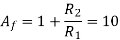
The voltage gain of the non-inverting amplifier is given as
Now assume the value of R1 to be 1KΩ and calculate the value R2 from the above equation.

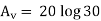
Hence for a voltage gain of 10, values of R1 and R2 are 1KΩ and 9KΩ respectively. Gain in dB is given as 20LogA = 20Log10 = 20dB
Now we are given with the cut-off frequency value as 175Hz and input impedance value as 20KΩ. By substituting these values in the equation and value of C can be calculated as follows.


Q2) Assume Rs1 = Rs2 = 15KΩ and capacitor C1 = C2 = 100nF. The gain resistors are R1=1KΩ, R2= 9KΩ, R3 = 6KΩ, and R4 =3KΩ. Design a second-order active low pass filter with these specifications.
A2)
The cut-off frequency is given as

(1)


The gain of first stage amplifier is


The gain of second stage amplifier is


Total Gain of the filter


The total gain in dB
(2) 
(3) 
The gain at cut-off frequency is
(4) Gain at 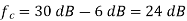
Q3) Consider cut-off frequency value as 10 KHz, pass band gain Amax as 1.5 and capacitor value as 0.02 µF.
A3)
The equation of the cut-off frequency is fC = 1 / (2πRC)
By re-arranging this equation,
We have R = 1 / (2πfC)
R = 1/ (2π * 10000 * 0.02 * 10-6) = 795.77 Ω
The pass band gain of the filter is Amax = 1 + (R3/R2) = 1.5
R3 = 0.5 R2
If we consider the R2 value as 10KΩ, then R3 = 5 kΩ
We can calculate the gain of the filter as follows:
Voltage Gain for High Pass filter :
| Vout / Vin | = Amax * (f/fc) /√[1 + (f/fc)²]
Av(dB) = 20 log10 (Vout/Vin)
Q4) Design a filter with cut-off frequency 4 KHz and the delay rate in the stop band is 40dB/decade. As the delay rate in the stop band is 40dB/decade we can clearly say that the filter is second order filter.
A4)
Let us consider the capacitor values as C1= C2 = C = 0.02µF
The equation of the cut-off frequency is fc = 1/ 2πRC Hz
By re-arranging this equation we have R = 1/ 2πfC
By substituting the values of cut-off frequency as 4 KHz and capacitor as 0.02µF
R = 1.989 KΩ = 2KΩ.
Let the gain of the filter is 1+ R1/R2 = 2
R1 / R2 = 1
R1 = R2
Therefore, we can take R1 = R2 = 10 KΩ
Thus, the obtained filter is shown as below:
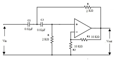
Fig 1 HPF Designed circuit
Q5) Consider the infinity gain multiple feedback active filter circuit for which the resonating frequency is 1.5 kHz, maximum Voltage gain is 15 and quality factor is 7.
A5)
Then component values are calculated as follows:
For Resistors
R1 =Q/ 2πfc CAmax
R2 = Q/ πfc C
And R3 = Q/ 2πfc C(2Q2 - Amax)
Choosing capacitor C1 =C2 =C = 0.02µF
Q= fc / Bandwidth = 0.5 √(R2/ R1) = 7
Applying values to R1, R2, R3 we get R1 = 2.47kΩ , R2 = 74.27 kΩ , R3 = 447.4 kΩ.
We consider that the changed resistor value as R3´ and the changed cut-off frequency value fc´=2 KHz then we can equate for the new resistor value as follows:
R3´ = R3 (fc/fc´)2 = 447.4(1.5/2)2 = 251.66 Ω
Therefore, simply by taking the required frequency we can calculate the new resistor value.
Q6) An active band pass filter that has a voltage gain Av of one (1) and a resonant frequency, ƒr of 1kHz is constructed using an infinite gain multiple feedback filter circuit. Calculate the values of the components required to implement the circuit.
A6)
Firstly, we can determine the values of the two resistors, R1 and R2 required for the active filter using the gain of the circuit to find Q as follows.
Av = 1 = -2Q2
QBP = √(1/2) =0.7071
Q = 0.7071 = 0.5 √(R1/R2)
Or R1/R2 =2
Then we can see that a value of Q = 0.7071 gives a relationship of resistor, R2 being twice the value of resistor R1. Then we can choose any suitable value of resistances to give the required ratio of two. Then resistor R1 = 10kΩ and R2 = 20kΩ.
The center or resonant frequency is given as 1kHz. Using the new resistor values obtained, we can determine the value of the capacitors required assuming that C = C1 = C2.
F1 = 1000 Hz = 
C =  =
=  =11.2nF
The closest standard value is 10nF.
Q7) Find the order of an active low pass Butterworth filter whose specifications are given as: Amax = 0.5dB at a pass band frequency (ωp) of 200 radian/sec (31.8Hz), and Amin = -20dB at a stop band frequency (ωs) of 800 radian/sec. Also design a suitable Butterworth filter circuit to match these requirements.
A7)
Firstly, the maximum pass band gain Amax = 0.5dB which is equal to a gain of 1.0593, remember that: 0.5dB = 20*log(A) at a frequency (ωp) of 200 rads/s, so the value of epsilon ε is found by:
1.0593 = =(1 + €2)1/2
€ = 0.3495
Secondly, the minimum stop band gain Amin = -20dB which is equal to a gain of 10 (-20dB = 20*log(A)) at a stop band frequency (ωs) of 800 rads/s or 127.3Hz.
Substituting the values into the general equation for a Butterworth filters frequency response gives us the following:
H(jw) = 1/ √(1+ €2(w/wp)2n)

(10)2 = 1 + 0.1221 x 42n
On solving this we get n = 2.42
Since n must always be an integer ( whole number ) then the next highest value to 2.42 is n = 3, therefore a “a third-order filter is required” and to produce a third-order Butterworth filter, a second-order filter stage cascaded together with a first-order filter stage is required.
From the normalised low pass Butterworth Polynomials table above, the coefficient for a third-order filter is given as (1+s)(1+s+s2) and this gives us a gain of 3-A = 1, or A = 2. As A = 1 + (Rf/R1), choosing a value for both the feedback resistor Rf and resistor R1 gives us values of 1kΩ and 1kΩ respectively as: ( 1kΩ/1kΩ ) + 1 = 2.
Q8) Design a basic wide-band, RC band stop filter with a lower cut-off frequency of 200Hz and a higher cut-off frequency of 800Hz. Find the geometric center frequency, -3dB bandwidth and Q of the circuit.
A8)
F = 1/ 2πRC
The upper and lower cut-off frequency points for a band stop filter can be found using the same formula as that for both the low and high pass filters as shown.
Assuming a capacitor, C value for both filter sections of 0.1uF, the values of the two frequency determining resistors, RL and RH are calculated as follows.
Low Pass Filter Section
FL = 1/ 2πRLC = 200Hz and C =0.1 µF
RL = 1/ 2π x 200 x 0.1 10 -6 = 7958Ω or 8kΩ
High Pass Filter Section
FH = 1/ 2πRHC = 800Hz and C =0.1 µF
RH = 1/ 2π x 800 x 0.1 10 -6 = 1990Ω or 2kΩ
From this we can calculate the geometric center frequency, ƒC as:
Fc = √(fL x fH) = √(200x 800) = 400 Hz
fBW = fH - fL = 800 – 200 =600 Hz
Q = Fc/ fBW = 400/600 = 0.67 OR -3.5 dB
If we make the op-amps feedback resistor and its two input resistors the same values, say 10kΩ, then the inverting summing circuit will provide a mathematically correct sum of the two input signals with zero voltage gain.
Then the final circuit for our band stop (band-reject) filter example will be:
Band Stop Filter Design
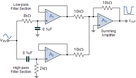
Fig 2 Band Stop Filter
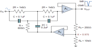
Q9) Design a two op-amp narrow-band, RC notch filter with a center notch frequency, ƒN of 1kHz and a -3dB bandwidth of 100 Hz. Use 0.1uF capacitors in your design and calculate the expected notch depth in decibels.
Data given: ƒN = 1000Hz, BW = 100Hz and C = 0.1uF.
A9)
1. Calculate value of R for the given capacitance of 0.1uF
R =  x 106
x 106
R = 795 Ω
2. Calculate value of Q
Q = FN/ fBW = 1000/100 =10
3. Calculate value of feedback fraction k
K = 1 – 1/4Q =1- 1/ 4x 10 = 0.975
4. Calculate the values of resistors R3 and R4
K = 0.975 = R4/(R3+R4)
Assuming R4 = 10kΩ then R3 is
R3 = R4 – 0.975 X R4
R3 =250Ω
5. Calculate expected notch depth in decibels, dB
1/Q =1/10 =0.1
fN(dB) = 20 log (0.1) = -20dB
Notch Filter Design
Q10) Design a second-order high-pass Sallen and Key Filter circuit with the following characteristics: ƒC = 200Hz, and Q = 3
A10)
To simplify the math’s a little, we will assume that the two series
Capacitors CA and CB are equal (CA = CB = C) and also the two
Resistors RA and RB are equal (RA = RB = R).
We will choose C=100nF

The calculated value of R is 7957Ω, so the nearest preferred value used is 8kΩ.
For Q = 3, the gain is calculated as:
If Q=3 then
If A = 2.667, then the ratio of R1/R2 = 1.667 as shown.

Assume a value of 
The calculated value of R2 is 5998Ω, so the nearest preferred value used 6000Ω or 6kΩ. This then gives us the final circuit for our Sallen and Key high-pass filter example of
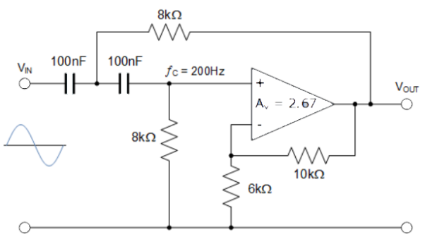
Fig 3. Sallen and Key High Pass Filter
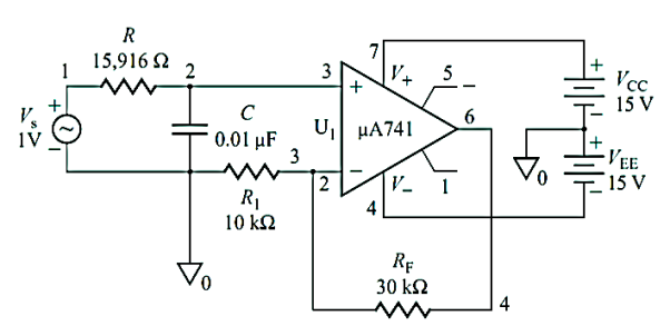
Q11) Design a first-order low-pass filter to give a high cut-off frequency of fo 1 kHz with a pass-band gain of 4. If the desired frequency is changed to fn 1.5 kHz, calculate the new value of Rn?
A11)
(a) The high cut-off frequency is fo 1 kHz. Choose a value of C less than or equal to 1 F: let C 0.01
 F. Using Equation below calculate the value of R
R =  x 106 = 15.916 k Ohm
Choose values of R1 and RF to meet the pass-band gain K
K= 1+RF ⁄ R1
RF ⁄ R1 = 4-1 =3
If we let R1=10 k Ohm, RF= 30kOhm
Calculate the frequency scaling factor, FSF =fo ⁄ fn
FSF = 1kHz/1.5kHz =0.67
Calculate the new value of Rn =FSF x R = 0.67 x 16000= 10.66kOhm
The LPF design is
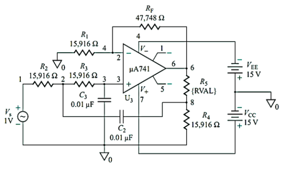
Q12) Design a second-order low-pass filter as in Fig. 12.14, to give a high cutoff frequency of fH =fo =1 kHz, a pass-band gain of K= 4, and Q =0.707, 1, 2, and infinity.
A12)
To simplify the design calculations, let R1= R2= R3= R4= R and let C2= C3= C. Choose a value of C less than or equal to 1 F: Let C= 0.01  F. For R2 =R3 =R and C2 =C3 =C
R=  x 106 = 15.916 kOhm
Then RF =(K -1)/R1= (4-1) x 15,916= 47,748 Ohm
For Q= 0.707 and K= 4, gives x =1.586 ⁄ K =1.586 ⁄ 4= 0.396.
R5/R4=1-x/x
Which, for x= 0.396 and R4= R= 15,916 Ohm
R5= 1.525 x 15,916= 24,275 Ohm
For Q= 1 and K= 4, gives 3-xK= 1 or x= 2 ⁄ K= 0.5
R5= R= 15,916 Ohm
For Q= 2 and K= 4, gives 3-xK= 1/2 or x= 2.5 ⁄ K= 0.625 Ohm
R5 = 0.6R = 9550 Ohm
For Q= infinity and K= 4, gives 3-xK= 1/Q=0 or x= 3 ⁄ K= 0.75 Ohm
R5 = 0.333R = 5305 Ohm
The design of LPF with above circuit parameters is shown below. This is a PSpice model
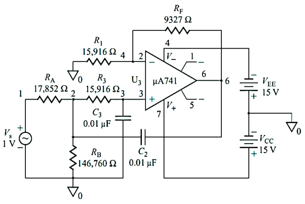
Q13) Designing a second-order low-pass Butterworth filter for |H(jωo)|= 1. Design a second-order Butterworth low-pass filter as in Figure below to yield H(jωo)= 1 (or 0 dB), a cutoff frequency of fo= 1 kHz, and Q= 0.707.

A13)
For the Butterworth response, Q= 0.707. From above example we have C= 0.01 F and R= 15,916
K = 3 – (1/ Q) = 3 – (1/ 0.707) = 1.586
RF = (K - 1)/R1 = (1.586 - 1) * 15,916 = 9327 
Ra = RK /3 - K = [15,916 * 1.586]/ [3 - 1.586] = 17,852 
Rb = RK /2K - 3 = [15,916 * 1.586]/ [(2 * 1.586) – 3] = 146,760 
|H(j0)|= 3 - K = 3 - 1.586 = 1.414
The design is shown below
Q14) Design a second-order high-pass filter as in Figure below, with a cut-off frequency of fo= 1 kHz, a pass-band gain of K 4, and Q 0.707, 1, 2, and infinity.
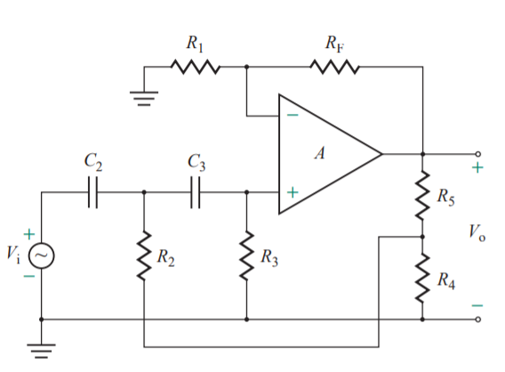
A14)
Since high-pass filters are formed simply by interchanging the Rs and Cs of the input RC network and since fo= 1 kHz, we can use the values of R and C that were determined for the second-order low-pass filter of Example above—that is, C= 0.01  F, and R4= R= 15,916
For Q= 0.707, R5= 24,275 
For Q= 1, R5= R= 15,916 
For Q 2, R5= 0.6R= 9550 
For Q=infinity, R5= 0.3333R= 5305 

Q15) Design a second-order Butterworth high-pass filter as in Figure below to yield |H(j∞)|= 1 (or 0 dB), a cutoff frequency of fo= 1 kHz, and Q= 0.707.
A15)
For Q= 0.707, and from above question we take C= 0.01  F, and R= 15,916
K = 3 – 1/ Q = 3 – 1/ 0.707 = 1.586
RF= (K - 1)/R1= (1.586 - 1) x 15,916= 9327 
Ca = C/ K = 0.01  F/ 1.586 = 6.305 nF
Cb = C(K - 1)/ K = 0.01  F * (1.586 - 1) /1.586 = 3.695 nF
Second-order high-pass Butterworth filter for PSpice simulation is below

Q16) Designing a wide-band-pass filter (a) Design a wide-band-pass filter with fL= 10 kHz, fH= 1 MHz, and a pass-band gain of KPB= 16. (b) Calculate the value of Q for the filter.
A16)
a) Let the gain of the high-pass section be KH= 4. For the first-order high-pass section, fL= 10 kHz
We let C= 1 nF
R=  x 109 = 15.915 k
KH= 1+RF/R1
4= 1+ RF/R1
RF/R1=3
If we let R1= 10 k  , RF= 3R1= 30 k
  . For the first-order low-pass section, fH= 1 MHz and the desired gain is KL= KPB ⁄ KH =16 ⁄ 4 =4
We let C′= 10 pF
R’=  x 1012=15.915 k
KL= 1+R’F/R’1
4= 1+ R’F/R’1
R’F/R’1=3
b) fC = √10 kHz * 1 MHz = 100 kHz
BW 1 MHz - 10 kHz= 990 kHz
Q = (100kHz)/1MHz-10kHz) = 0.101
The circuit for First-Order BPF is shown below.
Q17) In a transistor Hartley oscillator if L1 = 0.1 m H, L2 = 10  H and mutual inductance between the two coil M = 20
  H, calculate the value of capacitor C1 of oscillatory circuit to obtain frequency of 4110 kHz
A17)
L1 = 100  H
H
L2 = 10  H
H
M = 20  H
H
Total inductance, L = L1 + L2 + 2M
= 100 + 10 + 2 × 20
= 150  H
H
F = 
4110× 103 = 
 × 150 × 10-6 × C =
C = 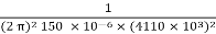 = 10pf
Q18) Find the operating frequency of a transistor Colpitt’s oscillator if C1 = 30 pf, C2 = 60Þf and L = 10  H
H
A18)
Total capacitance, CT =  =
=  = 20 pf = 20× 10-12 F
Inductance, L = 10 H = 10× 10-6 H
F = 
=  = 11.25 MH
Q19) Write difference between Active and Passive Filters?
A19)
Type of filter Passive filter Active filter
Advantages | No power supply required.
Can handle large currents and high voltages.
Very cheap. | Generally easier to tune. No inductors. Small in size and weight |
Disadvantages | Limited standard sizes, often requiring variable inductors and therefore tuning.
Generally not amenable to miniaturization. | Power supply require susceptible to inter modulation, oscillations |
Q20) What are phase shift oscillators explain using op-amp?
A20)
Phase Shift oscillator

In an RC Oscillator circuit, the input is shifted 180o through the feedback circuit returning the signal out-of-phase and 180o again through an inverting amplifier stage to produces the required positive feedback.
This then gives us “180o + 180o = 360o” of phase shift which is effectively the same as 0o, thereby giving us the required positive feedback.
In other words, the total phase shift of the feedback loop should be “0” or any multiple of 360o to obtain the same effect.
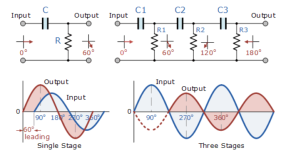
The circuit on the left shows a single resistor-capacitor network whose output voltage “leads” the input voltage by some angle less than 90o.
In a pure or ideal single-pole RC network. It would produce a maximum phase shift of exactly 90o, and because 180o of phase shift is required for oscillation, at least two single-poles networks must be used within an RC oscillator design.
However, in reality it is difficult to obtain exactly 90o of phase shift for each RC stage so we must therefore use more RC stages cascaded together to obtain the required value at the oscillation frequency.
The amount of actual phase shift in the circuit depends upon the values of the resistor (R) and the capacitor (C), at the chosen frequency of oscillations with the phase angle ( φ ) being given as:
Xc = 1/2π fc R=R
Z = [R 2 + Xc 2] ½
Ø = tan -1 Xc /R


