Unit - 5
Three-Phase Voltage Source Inverter
Q1) Draw and explain three phase voltage source inverter with waveform.
A1) For high power applications, three phase voltage source inverters are preferred to
Provide three phase voltage source in addition to that the magnitude, phase and frequency of voltages should be controlled.
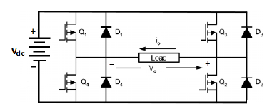
The typical three-phase VSI topology is shown in fig below, and middle points of the inverter legs are connected to three phase RL load. There are the eight valid switch states which are given in Table. The switches of any leg of the inverter (S1 and S4, S3 and S6 or S5 and S2) cannot be switched on simultaneously. Because it would result in short circuit across the DC link voltage supply. Similarly, the switches of any leg of the inverter cannot be switched off simultaneously to avoid undefined states in the VSI and thus undefined ac output line voltages.
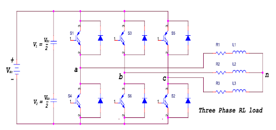
Fig: Power circuit of three phase voltage source inverter with RL load
Two of eight valid states (7 and 8) are called as zero switch states to produce zero AC line voltages. In this case, the AC line currents freewheel through either the upper or lower components. The remaining states (1 to 6 in Table) are called as non-zero switch states to produce non-zero AC output voltages. The resulting AC output line voltages consist of discrete values of voltages that are Vdc , 0, and - V dc for the topology shown in waveform figure below.

Fig: Output voltage waveform of three phase VSI
The pole voltages and output voltage waveforms obtained with respect to switching states from three phase VSI are shown in waveform. Analysis of three phase VSI is carried out in either 1200 mode or 1800 mode of conduction.
1800 conduction Mode
In this mode each switch turned on at every 600.Conduction of switches in each switching states, pole voltages measured at ‘a’ and ‘b’ and load voltage (Vab ) are noted in the Table below.
Q2) Explain switch state in Three-Phase Voltage Source Inverter.
A2)
S11 | S12 | S31 | Vab | Vbc | Vca |
0 | 0 | 0 | 0 | 0 | 0 |
0 | 0 | 1 | 0 | - VDC | VDC |
0 | 1 | 0 | - VDC | VDC | 0 |
0 | 1 | 1 | - VDC | 0 | - VDC |
1 | 0 | 0 | VDC | 0 | - VDC |
1 | 0 | 1 | VDC | -VDC | 0 |
1 | 1 | 0 | 0 | VDC | - VDC |
1 | 1 | 1 | 0 | 0 | 0 |
The inverter has eight switch states given in Table 4.1. As explained earlier in order that the circuit satisfies the KVL and the KCL, both of the switches in the same leg cannot be turned ON at the same time, as it would short the input voltage violating the KVL.
Thus, the nature of the two switches in the same leg is complementary.
In accordance to Figure
S11 + S12 = 1
S21 + S22 = 1
S31 + S32=1
Of the eight switching states as shown in Table two of them produce zero ac line voltage at the output. In this case, the ac line currents freewheel through either the upper or lower components. The remaining states produce no zero ac output line voltages. In order to generate a given voltage waveform, the inverter switches from one state to another. Thus, the resulting ac output line voltages consist of discrete values of voltages, which are -VDC, 0, and VDC.
The selection of the states in order to generate the given waveform is done by the modulating technique that ensures the use of only the valid states.
VDC/2 (S11 – S12) = Van + Vno
VDC/2 (S21 – S22) = Vbn + Vno
VDC/2(S31-S32) = Vcn + Vno
Q3) Write about instantaneous outputvoltages.
A3)
180° Conduction Mode
In this conduction mode, each device will be in conduction with 180° where they are activated at intervals with 60°. The output terminals like A, B, and C are connected to the star or 3 phase delta connection of the load.
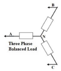
Figure. Balanced Load
The balanced load for three phases is explained in the following diagram. For 0 to 60 degrees, the switches like S1, S5 & S6 are in conduction mode. The load terminals like A & C are linked to the source on its positive point, whereas the B terminal is associated with the source on its negative point. Furthermore, the R/2 resistance is available among the two ends of neutral & the positive whereas R resistance is available among the neutral & the negative terminal.
In this mode, the voltages of load are given in the following.
VAN = V/3,
VBN = −2V/3,
VCN = V/3
The line voltages are given in the following.
VAB = VAN − VBN = V,
VBC = VBN− VCN = −V,
VCA = VCN− VAN = 0
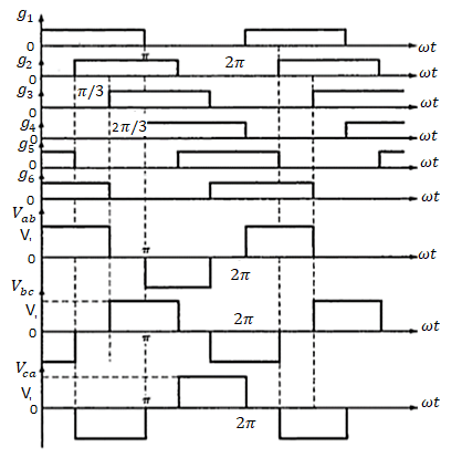
Figure. Output waveforms
120° Conduction Mode
In this type of conduction mode, every electronic device will be in a conduction state with 120°. It is apt for a delta connection within a load as it results within a six-step kind of waveform across one of its phases. So, at any instant, only these devices will conduct every device that will conduct at 120° only.
The connection of ‘A’ terminal on the load can be done through the positive end whereas the B terminal can be connected toward the negative terminal of the source. The ‘C’ terminal on the load will be in conduction is known as the floating state. Also, the phase voltages are equivalent to the voltages of load which is given below.
Phase voltages are equal to line voltages, so
VAB = V
VBC = −V/2
VCA = −V/2

Figure. Output Waveforms
Q4) Explain1800 Conduction Mode and 1200 Conduction Mode.
A4)
Modes of Operations
The three phase output can be obtained from a configuration of sixswitches and six diodes. Two types of control signals can be applied to theswitches: 180°conduction or 1200 conduction.
1800 Conduction Mode
In these inverters each switch conducts for a duration of 1800. Threeswitches remain on, at any instant of time. When switch-1 is switched on,terminal 'a' is connected to the positive terminal of the DC input voltage.
When switch-4 is switched on, terminal 'b' is connected to the negativeterminal of the DC source. There are six modes of operation in a cycle and the duration of each mode is 600.The switches are numbered in the sequence ofgating the switches 1-2-3, 2-3-4, 3-4-5, 4-5-6, 5-6-1, 6-1 -2. The gating signalsare shifted from each other by 600 to obtain three phase balanced voltages.
1200 Conduction Mode
In this conduction mode each switch conducts for 120". Only twoswitches remain on at any instant of time. The conduction sequence of switchesis 6-1, 1-2, 2-3,3-4,4-5, 5-6, and 6-1. There are three modes of operation in a half cycle and the equivalent circuits.


Fig: Phase current waveform
Q5) Explain three-phase sinusoidal pulse width modulation.
A5)
The voltage source inverter that use PWM switching techniques have a DC input voltage (VDC = VS) that is usually constant in magnitude. There are several techniques of Pulse Width Modulation (PWM). The efficiency parameters of an inverter such as switching losses and harmonic reduction are principally depended on the modulation strategies used to control the inverter.
The Sinusoidal Pulse Width Modulation (SPWM) technique has been used for controlling the inverter as it can be directly controlled the inverter output voltage and output frequency according to the sine functions.
SPWM techniques are characterized by constant amplitude pulses with different duty cycles for each period. The width of these pulses are modulated to obtain inverter output voltage control and to reduce its harmonic content.
In SPWM technique three sine waves and a high frequency triangular carrier wave are used to generate PWM signal.
Generally, three sinusoidal waves are used for three phase inverter. The sinusoidal waves are called reference signal and they have 1200 phase difference with each other.
The carrier triangular wave is usually a high frequency (in several KHz) wave. The switching signal is generated by comparing the sinusoidal waves with the triangular wave. The comparator gives out a pulse when sine voltage is greater than the triangular voltage and this pulse is used to trigger the respective inverter switches. In order to avoid undefined switching states and undefined AC output line voltages in the VSI, the switches of any leg in the inverter cannot be switched off simultaneously.
The phase outputs are mutually phase shifted by 1200 angles The ratio between the triangular wave & sine wave must be an integer N, the number of voltage pulses per half-cycle, such that, 2N= fc /fs.
Q6) A single phase half bridge inverter has a resistance of 2.5Ω and input DC voltage of 50V. Calculate the following
(a) the rms voltage
(b) the power output
(c) Peak current and average current
(d) Harmonic rms voltage
(e) THD
A6)
(a) The RMS voltage occurring at the fundamental frequency
E1RMS = 0.9 50 V = 45 V
b. The power Output
RMS output voltage = EORMS = E = 50 V
Output power = E2/R = (50)2/2.5 = 1000 W
c. Peak current and average current
Peak current IP= E0 /R = 50/2.5 = 20 A
Average current = IP/2 = 20/2 = 10 A
d. Harmonic RMS voltage
En= {(EORMS)2 – (E1RMS)2}0.5 = [502 – 452]0.5 = 21.8 V
e. Total harmonic distortion
En/E1RMS = 21.8/45 = 0.48 100% = 48%
Q7) The single-phase full-bridge inverter shown below is operated in the quasi-square-wave mode at the frequency f = 50 Hz with a phase-shift of β = 2π/3 between the half-bridge outputs vao and vbo. (a) Sketch the load voltage vo and find its total harmonic distortion (THD). (b) With a purely inductive load L= 50 mH, sketch the load current io and find its peak-to peak value Ipp.

A7)
(a)


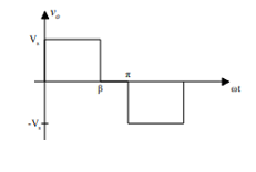
(b)
L di0/dt = Vs 0 ≤ t ≤ β/ i0(t) = -Ip + Vs/L t
t = β/ i0 – Ip Ip = - Ip + Vs/L β/
Ipp = 2Ip = β Vs/L = 2π/3 200/(100π 0.05) = 26.66 A

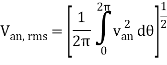
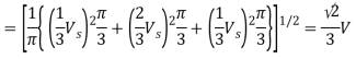
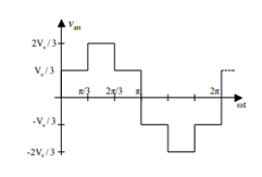
Q8) The three-phase half-bridge inverter shown below feeds a balanced Y-connected purely inductive load having inductance L per phase, and is operated in the square-wave mode (pole voltages are square waves) at the frequency f s. (a) Sketch phase-to-neutral voltage van (show all important voltage and time values) and find its rms value Van, rms. (b) Find the peak-to-peak value (Ipp) of the line current ia in terms of L and f

A8)
(a) van = 1/3 (2va0 – vb0 – vc0)
(b)

ia(t2) = ia(t) + 1/L  or in terms of angle ia(θ2) = ia(θ1) + 1/L
θ1 = 0, θ2 = π/3, van = 1/3 V, - I2 = - Ip + 1/L  I2 = Ip – πVs/9L
θ1 = π/3, θ2 = 2π/3, van = 2/3 Vs I2 = - I2 + 1/L  I2 = πVs/9L
Iw = 2Vp = 4πVs/9(2πfs)L = 2Vs/9fsL
Q9) The three-phase half-bridge inverter shown below feeds a balanced Y-connected resistive-inductive load with R = 10 Ω and L = 10 mH, and is operated in the square-wave mode (pole voltages are square waves) at frequency f s = 200 Hz
(a) Sketch phase a voltage van (show all important voltage and time values) and find its rms value.
(b) Find the amplitude of the fundamental component of the line current ia .

A9)
(a) As in Q.6
(b) Ia, 1 = Van, 1/|Z1| where, Van, 1 is the amplitude of the fundamental component of van and Z1 is the impedance of the load at the fundamental frequency.
Van, 1 can be found from the equation of van in terms of pole voltages:
Van = 1/3 (2va0 – vb0 – vc0) van, 1 = 2/3 va0, 1 – 1/3 vb0, 1 – 1/3 vc0, 1
va0, 1 = 2Vs/π sin(t) vb0, 1 = 2Vs/π sin (t – 120) vc0, 1 = 2Vs/π sin (t – 240)
van, 1 = 2Vs/π [ 2/3 sin(t) – 1/3 sin(t – 120) – 1/3 sin(t – 240)] = 2Vs/π sin (t ) Van, 1 = 2Vs/π = 127.32 V
Z1 = R + jL |Z1| = 
Ia, 1 = 7.93 A
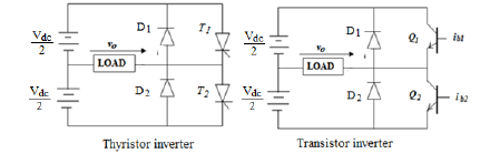
Q10) The single-phase half-bridge transistor inverter shown in Fig. Below has a resistive load of R = 3Ω and the d.c. Input voltage Vdc = 60 V. Determine:
(a) The rms value of the output voltage.
(b) The rms value of the load voltage at the fundamental frequency.
(c) The output power.
(d) The average and peak current of each transistor.
(e) The peak reverse blocking voltage VBR of each transistor.
(f) The total harmonic distortion factor.
A10)
(a) The rms value of the output voltage is

(b) The rms value of the load voltage at the fundamental frequency is
V01(rms) = c1/2 = 2/π Vdc = 0.45 Vdc = 0.45 60 = 27 V
(c) The output power is
P0 = (V01(rms))2/R = 302/3 = 300 W
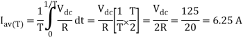
(d) The average and peak current of each transistor are
Ip = V0(rms)/R = 30/3 = 10A
Because each transistor conducts for a 50 % duty cycle, the average current of each transistor is
Iav = 10 0.5 = 5A
(e) The peak reverse blocking voltage VBR of each transistor is
VBR = 2 30 = 60V
(f) The total harmonic distortion factor is
THD = 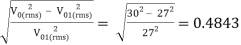
Q11) For the single-phase MOSFET bridge inverter circuit shown below, the source Vdc =125 V, load resistance R =10 Ω and output voltage frequency fo= 50 Hz.
a) Draw the output voltage and load current waveforms.
(b) Derive the rms value of the output voltage waveform and hence calculate the output power Po in terms of the output voltage.
(c) Analyse the amplitude of the Fourier series terms of the output voltage waveform by considering up to the 7th order harmonic. Determine the value of the rms output voltage in terms of harmonics rms values.
(d) Calculate the average and peak currents of each transistor.
(e) Estimate the total harmonic distortion factor THD of the circuit.
A11)
(a)

(b) The rms value of the output voltage is

P0 = V0(rms)2 = 1252/10 = 1562.5 W
(c) The Fourier series of the output voltage is
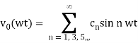
The amplitude cn of the nth harmonic is:
cn = 4Vdc/nπ = (4 125)/nπ = 159.12/n
v0(wt) = c1 sin t + c2 sin 3 t + c5 sin 5 t + c7 sin 7 t
= 159.12/1 sin t + 159.12/3 sin 3t + 159.12/5 sin 5t + 159.12/7 sin 7 t
Hence the output voltage Fourier representation is,
v0(t) = 159.12 sin t + 53.04 sin 3 t + 31.82 sin 5 t + 22.73 sin 7 t
In terms of the harmonics :

This value is less than V0(rms) since we calculate up to 7th order harmonics only.
(d) Since the duty cycle of each transistor is 0.5, the current waveform is as shown below

Peak current
Vdc/R = 125/10 = 12.5 A
(e) The total harmonic distortion factor:
V01(rms) = c1/2 = 159.12/2 = 112.6 V
THD = 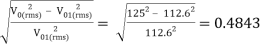
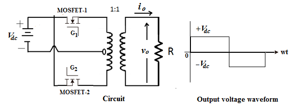
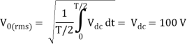
Q12) A single-phase MOSFET parallel inverter has a supply d.c. Voltage of 100V supplying a resistive load with R =10 Ω via a center-tap transformer with 1:1 ratio. The output frequency is 50 Hz.
(a) Draw the circuit diagram and the output voltage waveform of the inverter.
(b) Determine the rms value of the output voltage waveform.
(c) Determine the amplitude of the Fourier series terms for the square output voltage waveform up to 9th order harmonics.
(d) Calculate the rms value of the output voltage in terms of harmonic components that obtained in (b).
(e) Determine the power absorbed by the load consider up to 9th order harmonic.
(f) Draw the frequency spectra of the output voltage waveform.
(g) Calculate the total harmonic distortion factor THD.
A12)
(a) the circuit diagram and the output voltage waveform of the inverter
(b) The rms value of the output voltage is
(c) the Fourier series of the output voltage is
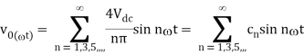
The amplitude cnof the n th order harmonic is:
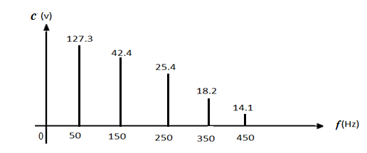
cn = 4Vdc/nπ = (4 100)/nπ = 127.3/n
v0(t) = c1 sin t + c3 sin 3 t + c5 sin 5 t + c7 sin 7 t + c9 sin 9 t
= 127.3/1 sin t + 127.3/3 sin 3t + 127.3/5 sin 5t + 127.3/7 sin 7 t + 127.3/9 sin 9 t
Hence the output voltage Fourier representation is,
v0(t) = 127.3 sin t + 42.4 sin 3 t + 25.5 sin 5 t + 18.2 sin 7 t
(d) In terms of the harmonics , the rms value of the output voltage is

(e) To calculate the power we most calculate the rms value of the current for each harmonic the amplitude of the nth harmonic current
In = cn/Zn
Where Zn = (R2 + (nL)2) = R
Pn = In(rms)2 R = (In/2)2 R
n | fn(Hz) | cn(V) | Zn(Ω) | In(A) | Pn(W) |
1 | 50 | 127.3 | 10 | 12.73 | 810 |
3 | 150 | 42.4 | 10 | 4.24 | 89.8 |
5 | 250 | 25.5 | 10 | 2.55 | 32.5 |
7 | 350 | 18.2 | 10 | 1.82 | 16.5 |
9 | 450 | 14.1 | 10 | 1.41 | 9.99 |
The total power is 
(f) The frequency spectrum is given in Fig.
(g) The total harmonic distortion factor
V0(rms) 100 V
V01 (rms) = c/2 = 127.3/ = 90 V
THD = 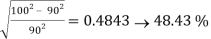
This is very high THD, the practical value of THD is about (3-10)% hence we need to use low-pass filter at the output to filter out most of the undesirable harmonic component and to produce nearly sinusoidal output waveform.


