Unit - 4
Single-Phase Voltage Source Inverter
Q1) Differentiate between voltage source inverter and Current source Inverter
A1)
Comparison between VSI and CSI
Current Source Inverter | Voltage Source Inverter |
|
|
2. A CSI is capable of withstanding short circuit across any two of it output terminals. Hence complementary short circuit on load and misfiring of switches are acceptable | 2. A VSI cannot accept the misfiring of switches. |
3. CSI is used in only buck or boost operation of inverter. | 3. VSI is used in only a buck or boost operation of inverter. |
4. The main circuit cannot be interchangeable. | 4. The main circuit cannot be interchanged here also. |
5. It is affected by the EMI noise. | 5. It is also affected by the EMI noise. |
Q2) What is function of Inverter? Explain single phase half wave inverter.
A2) A device that converts dc power into ac power at desired output voltage and frequency is called as Inverters. Inverters has wide range of applications such as adjustable AC speed drives, Uninterruptible Power Supplies (UPS), shunt active power filter, etc.
Inverters are classified into two types: (a) voltage source inverters and (b) current source inverters. If a DC input is a voltage source, then the inverter is called a
Voltage Source Inverter (VSI). Similarly in case of a Current Source Inverter
(CSI), the input to the circuit is a current source.
According to a number of phases, inverters are classified into two types
1. Single Phase Voltage Source Inverter
2. Three Phase Voltage Source Inverter
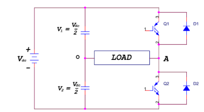
Figure shows a circuit topology of a Half-Bridge VSI, where two large capacitors are required to provide a neutral point O, such that each capacitor maintains a constant voltage (V1 = V 2=Vdc/2). Due to reason that the current harmonics produced by the operation of the inverter are low-order harmonics, a set of large capacitors (C1 and C2) are required. In this circuit, it has a single leg with two power switches Q1 and Q2. For bidirectional flow of current, feedback diodes 1D and D2 are employed in parallel with switches Q1 and Q2.
According to above figure, it is clear that both switches cannot be ON simultaneously, because both are directly connected across the DC link source.
If two switches conduct at the same time, a short circuit across the DC link
Voltage source dc V would be produced. There are two defined switching states
(States 1 and 2) as shown in Table below. In order to avoid the short circuit across the DC bus and the undefined AC output voltage condition, the modulating technique should make sure that at any moment either the top or the bottom switch of the inverter leg is on.
In a half bridge inverter, the input DC voltage is split in two equal parts (V1 and V2) through an ideal and loss-less capacitive potential divider. In the, it consists of one leg (one pole) of switches whereas the full bridge inverter has two such legs.
Each of these switches consists of an IGBT type controlled switch across which, an uncontrolled diode is put in anti-parallel approach. These switches are capable of conducting bi-directional current, but they have to obstruct only one polarity of voltage. In this type, the single phase load is connected between the mid-point of the input DC supply and the junction point of the two switches. These points are marked as ‘O’ and ‘A’ respectively.
Q3) Explain Switch states and instantaneous output voltage of Single-Phase Voltage Source Inverter.
A3) Switch states and instantaneous output voltage
State | Switching State | Output Voltage |
1 | Q1 is ON and Q2 is OFF | Vdc/2 |
2 | Q1 is OFF and Q2 is ON | - Vdc/2 |
With refer to the above Table, there are two switching states and the output voltage is obtained or produced on single phase load from either upper half DC voltage (Vdc/2) or lower half DC voltage (-Vdc/2). Principle and operation of this inverter with switching states are discussed below.
State 1
In state 1, upper half dc voltage (V1=Vdc/2) and power switch Q1 are in conducting mode and remaining components are in non-conducting mode. During time period of 0 to T/2, Switch Q1 is on and upper voltage (Vdc/2) is appeared across a load as an output voltage (VAO).
State 2
In state 2, lower half DC voltage (V2=Vdc/2) and power switch Q2 are in conduction mode and remaining components are in non- conduction mode. During time period from (T/2) to T, switch Q2 is on and lower voltage (V2=Vdc/2) is obtained across a load as an output voltage. Due to reverse polarity, output voltage (Aov) is negative.
During the time interval 0 to (T/2) to T, (Aov) acquires a magnitude of (Vdc/2) when Q1 is turned on and the magnitude reverses to ( - Vdc/2) ,when Q2 is turned on for the period (T /2) to T.

Fig: Output waveform of half bridge Inverter
Q4) What is square wave Inverter? Explain in detail
A4) A single-phase square wave type voltage source inverter produces square shaped output voltage for a single-phase load. Such inverters have very simple control logic and the power switches need to operate at much lower frequencies. Power circuits of half wave and full wave bridge inverters are redrawn in Fig(a) and (b) below.

Fig(a) single phase half wave bridge VSI, fig(b) single phase full wave bridge VSI
Here we both circuits are analysed under the assumption of ideal circuit conditions. Means it is assumed that the input dc voltage (Edc) is constant and the switches are lossless. In half bridge topology the input dc voltage is split in two equal parts through an ideal and loss-less capacitive potential divider.
The half bridge topology consists of one leg (one pole) of switches whereas the full bridge topology has two such legs. Each leg of the inverter consists of two series connected electronic switches shown within dotted lines in the figures.
Each of these switches consists of an IGBT type controlled switch across which an uncontrolled diode is put in anti-parallel manner. These switches are capable of conducting bi-directional current but they need to block only one polarity of voltage. The junction point of the switches in each leg of the inverter serves as one output point for the load.
In half bridge topology the single-phase load is connected between the mid-point of the input dc supply and the junction point of the two switches (in Fig. (a) These points are marked as ‘O’ and ‘A’ respectively).
For ease of understanding, the switches Sw1 and Sw2 may be assumed to be controlled mechanical switches that open and close in response to the switch control signal.
Now, if the switches Sw1 and Sw2 are turned on alternately with duty ratio of each switch kept equal to 0.5, the load voltage (VAO) will be square wave with a peak-to-peak magnitude equal to input dc voltage (Edc).

Fig: Output voltage of half bridge inverter
The above Fig. Shows a typical load voltage waveform output by the half bridge inverter. VAO acquires a magnitude of +0.5 Edc when Sw1 is on and the magnitude reverses to -0.5 Edc when Sw2 is turned on.
The two switches of the inverter leg are turned on in a complementary manner. For a general load, the switches should neither be simultaneously on nor be simultaneously off. Simultaneous turn-on of both the switches will amount to short circuit across the dc bus and will cause the switch currents to rise rapidly.
For an inductive load, containing an inductance in series, one of the switches must always conduct to maintain continuity of load current.
Q5) Explain sinusoidal pulse width modulation.
A5) There are many inverter topologies but output current distortion and efficiency are the two main parameters for the selection of inverters. The unipolar and bipolar inverters uses SPWM (Sinusoidal Pulse Width Modulation) technique.
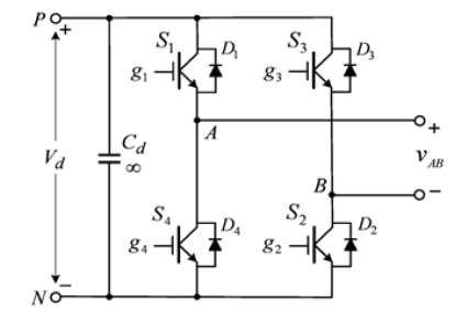
Fig: Single phase H-bridge Inverter
The output waveform (VAB) of switches between positive and negative dc voltages this scheme is called bipolar PWM. The unipolar modulation normally requires two sinusoidal modulating waves’ vm and vm- which are of same magnitude and frequency but 1800 out of phase.
The H-Bridge inverter topologies (both unipolar and bipolar) are made up of power electronic switches and are fed with constant amplitude pulses with varying duty cycle for each period. The SPWM pulses are generated by comparison of two waves- a carrier wave, which is triangular in this case and a modulating reference wave whose frequency is the desired frequency, which is sinusoidal in this case.
This pulse width modulation inverter is characterized by simple circuitry and rugged control scheme that is SPWM technique to obtain inverter output voltage control and to reduce its harmonic content.
Bipolar PWM inverter
In the above fig, the upper and the lower switches in the same inverter leg work in a complementary manner with one switch turned on and other turned off. Thus we need to consider only two independent gating signals vg1 and vg3 which are generated by comparing sinusoidal modulating wave vm and triangular carrier wave vcr. The inverter terminal voltages are obtained denoted by VAN and VBN and the inverter output voltage VAB = VAN-VBN. Since the waveform of VAB switches between positive and negative dc voltages this scheme is called bipolar PWM.
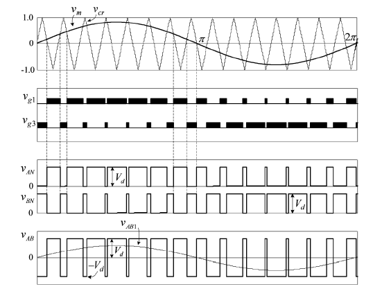
Fig: Waveform of Bipolar modulation scheme
UNIPOLAR PWM INVERTER
The unipolar modulation normally requires two sinusoidal modulating waves’ vm and -vm which are of same magnitude and frequency but 1800 out of phase. The two modulating wave are compared with a common triangular carrier wave vcr generating two gating signals vg1 and vg3 for the upper two switches S1 and S3.
It is observed that the upper two devices do not switch simultaneously, which is distinguished from the bipolar PWM where all the four devices are switched at the same time. The inverter output voltage switches between either between zero and +Vd during positive half cycle or between zero and –Vd during negative half cycle of the fundamental frequency thus this scheme is called unipolar modulation. The unipolar switched inverter offers reduced switching losses and generates less EMI.
On efficiency grounds, it appears that the unipolar switched inverter has an advantage.
Q6) Explain Concept of average voltage over a switching cycle
A6)
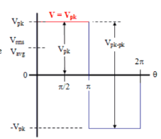
Figure. Square Wave
As the name implies, Vavg is calculated by taking the average of the voltage in an appropriately chosen interval. In the case of symmetrical waveforms like the square wave, a quarter cycle faithfully represents all four quarter cycles of the waveform. Therefore, it is acceptable to choose the first quarter cycle, which goes from 0 radians (0°) through π/2 radians (90°).
As with the Vrms formula,
Vavg = 1/π/2  . d
. d = 2/ π . Vpk
  | 0π/2
= 2/π .Vpk (π/2 -0) = Vpk
So, Vavg = Vpk
Q7) Explain Modulation index and output voltage.
A7)
Modulation index is the ratio of peak magnitudes of the modulating waveform and the carrier waveform. It relates the inverter’s dc-link voltage and the magnitude of pole voltage (fundamental component) output by the inverter.
In a pulse width modulated inverter the desired sine-wave output (the modulation) is modulated onto a high frequency square wave (the carrier). This can be done using a high speed digital signal processor but the traditional approach using a Comparator to perform the modulation is perhaps easier to understand.

The amplitude modulation index is defined as:

This will typically be less than one. An amplitude modulation index of more than 1 is possible but this leads to distortion of the output sine wave and in the extreme leads to a square wave output.
When V^control is above V^tri the output is +Vd. When V^controll is below V^tri the output is –Vd. The average output voltage (for this small increment of time) can be

V0=Vd.ma


