Unit - 2
Basic Computer Organization
Q1) Explain instruction codes?
A1) A program, on the other hand, is a set of instructions that specify the operations, operands, and the order in which processing must occur, as we all know. An instruction code is a set of bits that instructs the computer to carry out a specified task.
Instruction code: operation code
An instruction's operation code is a set of bits that describe operations like add, subtract, multiply, shift, and compliment. The total number of operations accessible on the computer determines the amount of bits necessary for the operation code. For a given 2^n operation, the operation code must be at least n bits long. An instruction code's operation section describes the operation to be done.
Instruction Code: Register Part
The procedure must be carried out on the data in the registers. As a result, an instruction code describes not only the operations to be executed, but also the registers where the operands (data) will be found and the registers where the result will be put.
Stored Program Organisation
The most basic approach to structure a computer is to have a two-part Processor Register and instruction code. The first component describes the action to be done, while the second part gives the address to be used. The memory address specifies the location of the operand in memory.
Data is kept in one area of memory while instructions are kept in another.
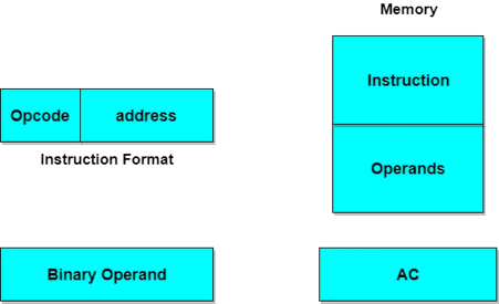
Accumulators are computers that have only one processor register (AC). The memory operand and the content of AC are used in the operation.
Common Bus System
There are eight registers, a memory unit, and a control unit in a basic computer. To move data from one register to another, paths must be supplied. The use of a Common Bus System is an efficient approach for exchanging data in a system. The common bus connects the output of registers and memory.
Load (LD)
The lines from the common bus are connected to the register inputs and memory data inputs. During the next clock pulse transition, the data from the bus is received by the register with the enabled LD input.
Let's start with the operand address sections before moving on to instruction forms.
When the operand is specified in the second half of an instruction code, the instruction is said to have instantaneous operand. When the address of an operand is specified in the second half of the instruction code, the instruction is said to have a direct address. The second portion of the instruction code, indirect address, indicates the address of a memory word in which the operand's address is found.
Q2) What are computer instructions?
A2) A computer instruction is a binary code that controls how a computer performs micro-operations in a series. They, together with the information, are saved in the memory. Every computer has its own set of instructions.
Operation codes (Opcodes) and Address are the two elements that they are divided into. Opcodes define how specific instructions should be executed. The registers or regions that can be used for that activity are determined by an address. Operands are specific components of computer instructions that specify what data should be processed.
Because the memory contains 4096 words, it requires 12 bits of memory to define the address. The addressing mode is determined by the instruction's 15th bit (where direct addressing corresponds to 0, indirect addressing corresponds to 1). As a result, the instruction format contains 12 bits of address and 1 bit for addressing mode, leaving 3 bits for Opcodes.
There are three different types of instruction codes in a basic computer. The instruction's operation code (opcode) is 3 bits long, with the remaining 13 bits depending on the operation code encountered.
There are three different formats to choose from.
1.Memory Reference Instruction
It specifies the address with 12 bits and the addressing mode with 1 bit (I). For direct addresses, I equals 0 while for indirect addresses, I equals 1.
2.Register Reference Instruction
The opcode 111 with a 0 in the leftmost bit of the instruction recognizes these instructions. The remaining 12 bits specify the procedure to be carried out.
3.Input-Output Instruction
The operation code 111 with a 1 in the leftmost bit of instruction recognizes these instructions. The input-output action is specified using the remaining 12 bits.
Q3) Write the different types of instruction codes in basic computer?
A3) There are three different formats to choose from.
1.Memory Reference Instruction
It specifies the address with 12 bits and the addressing mode with 1 bit (I). For direct addresses, I equals 0 while for indirect addresses, I equals 1.
2.Register Reference Instruction
The opcode 111 with a 0 in the leftmost bit of the instruction recognizes these instructions. The remaining 12 bits specify the procedure to be carried out.
3.Input-Output Instruction
The operation code 111 with a 1 in the leftmost bit of instruction recognizes these instructions. The input-output action is specified using the remaining 12 bits.
Q4) Define timing and control?
A4) A master clock generator controls the time of all registers in the basic computer. The clock pulses are applied to all of the system's flip-flops and registers, including the control unit's flip-flops and registers. The state of a register is not changed by clock pulses unless the register is enabled by a control signal. The control signals are generated in the control unit and provide control inputs for the common bus multiplexers, processor register control inputs, and accumulator microoperations.
Control organizations can be divided into two categories:
● Hardwired control and
● Microprogrammed control.
Hardwired Control
Gates, flip-flops, decoders, and other digital circuits are used to build the control logic. It has the advantage of being able to be optimized for a quick mode of operation. Control information is stored in a control memory in a microprogrammed structure. The control memory is programmed to start the needed microoperation sequence. If the design needs to be upgraded or changed, a hardwired control necessitates adjustments in the wiring among the various components, as the name implies.
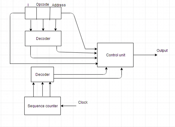
Fig 1: Hardwired control
Microprogrammed Control Unit
It's done through a programming approach. A program made up of micro-instructions is used to carry out a series of micro operations. Any alterations or changes in this organization can be made by the programmer altering the micro program in the control memory.

Fig 2: Microprogrammed control unit
● The address of the micro-instruction is specified in the Control memory address register.
● All control information is permanently saved in the control memory, which is considered to be a ROM.
● The microinstruction fetched from memory is stored in the control register.
● A control word in the micro-instruction specifies one or more micro-operations for the data processor.
● The next address is computed in the next address generator circuit and then transferred into the control address register to read the next microinstruction when the micro-operations are being executed.
● Because it determines the address sequence received from control memory, the next address generator is also known as a microprogram sequencer.
Q5) Explain about the instruction cycle?
A5) A program residing in the memory unit of a computer consists of a sequence of instructions. These instructions are executed by the processor by going through a cycle for each instruction.
In a basic computer, each instruction cycle consists of the following phases:
● Fetch the instruction from memory.
● Decode the instruction.
● Read the effective address from memory.
● Execute the instruction.
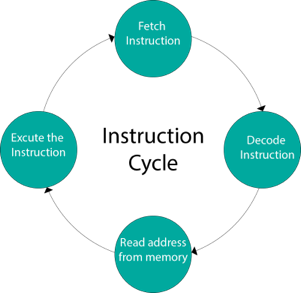
Fig 3: Input-Output Configuration
In computer architecture, input-output devices act as an interface between the machine and the user.
Instructions and data stored in the memory must come from some input device. The results are displayed to the user through some output device.
The following block diagram shows the input-output configuration for a basic computer.
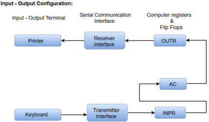
Fig 4: I/O configuration
● The input-output terminals send and receive information.
● The amount of information transferred will always have eight bits of an alphanumeric code.
● The information generated through the keyboard is shifted into an input register 'INPR'.
● The information for the printer is stored in the output register 'OUTR'.
● Registers INPR and OUTR communicate with a communication interface serially and with the AC in parallel.
● The transmitter interface receives information from the keyboard and transmits it to INPR.
● The receiver interface receives information from OUTR and sends it to the printer serially.
Design of a Basic Computer
A basic computer consists of the following hardware components.
● A memory unit with 4096 words of 16 bits each
● Registers: AC (Accumulator), DR (Data register), AR (Address register), IR (Instruction register), PC (Program counter), TR (Temporary register), SC (Sequence Counter), INPR (Input register), and OUTR (Output register).
● Flip-Flops: I, S, E, R, IEN, FGI and FGONote: FGI and FGO are corresponding input and output flags which are considered as control flip-flops.
● Two decoders: a 3 x 8 operation decoder and a 4 x 16 timing decoder
● A 16-bit common bus
● Control Logic Gates
● The Logic and Adder circuits are connected to the input of AC.
Q6) Describe memory reference instruction?
A6) It is vital to declare the function that each instruction is meant to execute in order to specify the microoperations required for its execution. The description of several commands is confusing. This is due to the fact that a written explanation of an instruction is usually extensive, and there isn't enough room in the table for such a lengthy explanation.
Register transfer notation can be used to precisely define the function of memory-reference instructions.
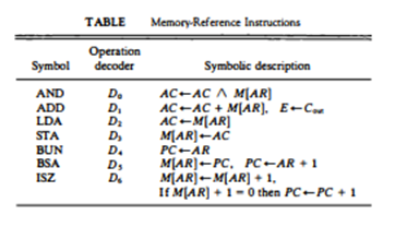
Fig 5: Memory reference instruction
The table contains the decoded D; for I = 0, 1, 2, 3, 4, 5, and 6 from the operation decoder for each instruction. The instruction's effective address is in the address register AR, which was set during timing signal T2 when I = 0 or timing signal T3 when I = 1. The memory-reference instructions are started with the timing signal T4• The symbolic description of each instruction in terms of register transfer notation is described in the table.
A series of micro operations will be required to execute the instruction in the bus system. This is due to the fact that data stored in memory cannot be directly processed. The data must be read from memory into a register, where logic circuits can be used to manipulate it. We'll now go through how each instruction works and identify the control functions and micro operations required to carry it out.
AND to AC
The AND logic operation is performed on pairs of bits in AC and the memory word indicated by the effective address in this instruction. The outcome of
AC is now in charge of the business. This instruction is carried out using the following micro operations:
D0T4: DR <- M [AR]
D0T5: AC <- AC /\ DR, SC <--- 0
The operation decoder D0 is used as the control function for this instruction since this output of the decoder is active when the instruction has an AND operation with the binary code 000. To carry out the instruction, two timing signals are required. The operand is transferred from memory to DR via the clock transition associated with timing signal T4. The result of the AND logic operation between the contents of DR and AC is transferred to AC by the clock transition associated with the following timing signal T5. During the same clock transition, SC is cleared to 0, and control is transferred to timing signal T0 to begin a new instruction cycle.
ADD to AC
The content of the memory word given by the effective address is added to the value of AC in this instruction. The output carry Cout is sent to the E (extended accumulator) flip-flop, and the total is transmitted to AC. The following rnicro operations are required to carry out this instruction:
D1T4: DR← M[AR]
D1T5: AC← AC + DR, E← Cout, SC ← 0
Same T and T5 are employed again, but this time with operation decoder D1 rather than D0, which was used for the AND instruction. Only one output of the operation decoder is active once the instruction is read from memory and decoded, and that output controls the sequence of microoperations that the control follows during the execution of a memory-reference instruction.
LDA: Load to AC
The memory word given by the effective address is transferred to AC using this instruction. The following micro operations are required to carry out this instruction:
D2T4: DR← M [AR]
D2T5: AC← DR, ← 0
Returning to the transportation system depicted in Fig. 5-4, we can see that there is no straight route from the bus to AC. The DR sends data to the adder and logic circuit, which can then be converted to AC. As a result, the memory word must first be read into DR, and then the content of DR must be transferred into AC. The delay in the adder and logic circuit is the reason for not connecting the bus to the AC inputs. It is expected that the time it takes to read a word from memory and transfer it across the bus, adder, and logic circuit is more than one clock cycle. We can keep one clock cycle every micro operation by not connecting the bus to the AC inputs.
STA: Store AC
The content of AC is stored in the memory word indicated by the effective address with this instruction. We may execute this instruction with one micro operation since the AC output is applied to the bus and the data input of memory is connected to the bus:
D3T4: M [AR] ← AC, SC ← 0
BUN: Branch Unconditionally
This instruction directs the program to the effective address-specified instruction. Remember that the address of the instruction to be read from memory in the next instruction cycle is stored in PC. The address of the next instruction in the program sequence is prepared by incrementing PC at time T1. The BUN instruction allows the programmer to define an out-of-sequence instruction, and we refer to this as unconditional branching (or jumping). One microoperation is used to carry out the instruction:
D4T4: PC ← AR, SC ← 0
The effective address from AR is communicated to PC via the common bus. The following instruction is then fetched and executed from the memory address specified by the new value in PC after SC is reset to 0.
BSA: Branch and Save Return Address
This instruction is useful for branching to a subroutine or function within the program. The BSA instruction stores the address of the next instruction in sequence (which is available in PC) in a memory location defined by the effective address when it is executed. The effective address plus one is subsequently sent to the PC and used as the address for the subroutine's first instruction. The following register transfer was described in Table 5-4 for this procedure.
M[AR] <-- PC, PC <-- AR + I
ISZ: Increment and Skip if Zero
The word defined by the effective address is incremented, and if the incremented value is equal to 0, PC is incremented by one. In the memory word, the programmer commonly stores a negative number (in 2's complement). This negative integer will eventually reach zero if it is repeatedly incremented by one. In order to bypass the following instruction in the program, PC is incremented by one at that point.
Because a word cannot be incremented within the memory, the word must be read into DR, incremented, and then stored back into memory. This is accomplished by doing the following series of microoperations:
D6T4: DR <-- M [AR]
D6T5: DR <-- DR + 1
D,T,: M [AR] <-- DR,
If (DR = 0) then (PC ← PC + 1), SC ← 0
Q7) Describe a complete computer?
A7) The basic computer's final flowchart of the instruction cycle, which includes the interrupt cycle. During the indirect or execute phases, the interrupt flip-flop R can be set at any time. After SC is cleared to 0, control returns to the timing signal T0. The computer enters an interrupt cycle if R = 1. The computer runs through an instruction cycle if R = 0. If the instruction is a memory-reference instruction, the computer checks for an indirect address before continuing to execute the decoded instruction. If the instruction is a register-reference instruction, one of the micro operations is used to execute it. It is executed with one of the micro operations if it is an input-output instruction.
Instead of using a flowchart, we can use a list of register transfer statements to describe the computer's operation. This is accomplished by gathering all control functions and micro operations into a single table.
The register transfer statements in this table describe the internal organization of the basic computer in a straightforward manner. They also provide all of the information required for the design of the computer's logic circuits.
Q8) How to design a basic computer?
A8) The following hardware components make up a basic computer:
1. A memory unit of 4096 words, each of which is 16 bits long.
2. AR, PC, DR, AC, IR, TR, OUTR, INPR, and SC are the nine registers.
3. I, S, E, R, lEN, FGI, and FGO are the seven flip-flops.
4. Two decoders: a three-by-eight operation decoder and a four-by-sixteen timing decoder
5. A 16-bit universal bus
6. Logic gates for control
7. Connected to the AC input is an adder and a logic circuit.
The memory unit is a common component that may be easily purchased from a commercial supplier. The registers are of the type seen in the diagram, are identical to the 74163 integrated circuit. The flip-flops might be of the D or JK variety. In a design similar to the one, a common bus system can be built with sixteen 8 x 1 multiplexers. We'll now demonstrate how to create control logic gates.

Fig 6: Flowchart for computer operations
Q9) What do you mean by input output?
A9) A computer can't do anything helpful until it can communicate with the outside world. In order for instructions and data to be stored in memory, they must come from some sort of input device. The user must be able to see the results of the computation via an output device. Many different types of input and output devices are used in commercial computers. We'll use a terminal unit with a keyboard and printer as an example to show the most fundamental requirements for input and output connectivity.
Input-Output Configuration
Serial data is sent and received by the terminal. Each quantity of data has an alphanumeric code of eight bits. The serial data from the keyboard is sent to the INPR input register. The output register OUTR stores the serial information for the printer. These two registers connect serially with a communication link and in parallel with the AC. Serial data from the keyboard is received by the transmitter interface and sent to INPR. The receiver interface accepts data from the OUTR and sends it serially to the printer. The input-output configuration is shown in Fig.
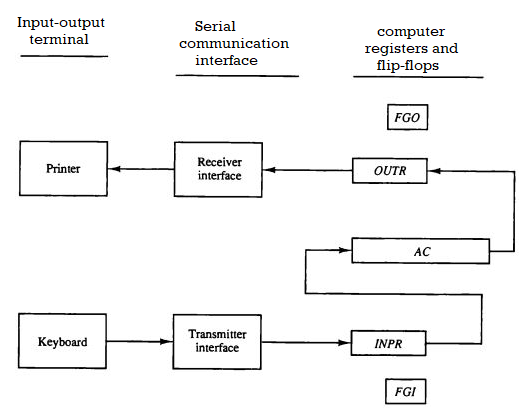
Fig 7: Input output configuration
Input register:
The input register INPR is an eight-bit register that stores alphanumeric input data. The control flip-flop FGI is a 1-bit input flag. When new information is available in the input device, the flag bit is set to 1 and cleared when the information is acknowledged by the computer. The flag is required to synchronize the input device's and computer's timing rate differences. The following is the information transfer procedure. The input flag FGI is initially set to 0. An 8-bit alphanumeric code is shifted into INPR and the input flag FGI is set to 1 when a key is pressed on the keyboard.
The information in INPR cannot be modified by pressing another key while the flag is set. If the flag bit is 1, the information from INPR is sent in parallel into AC, and FGI is cleared to 0. After the flag has been cleared, new data can be entered into INPR by pressing another key.
Q10) Define interrupt?
A10) Interrupt is a signal emitted by hardware or software when a process or an event needs immediate attention. It alerts the processor to a high priority process requiring interruption of the current working process. In I/O devices one of the bus control lines is dedicated for this purpose and is called the Interrupt Service Routine (ISR).
When a device raises an interrupt at let’s say process i, the processor first completes the execution of instruction i. Then it loads the Program Counter (PC) with the address of the first instruction of the ISR. Before loading the Program Counter with the address, the address of the interrupted instruction is moved to a temporary location. Therefore, after handling the interrupt the processor can continue with process i+1.
While the processor is handling the interrupts, it must inform the device that its request has been recognized so that it stops sending the interrupt request signal. Also, saving the registers so that the interrupted process can be restored in the future, increases the delay between the time an interrupt is received and the start of the execution of the ISR. This is called Interrupt Latency.
Hardware Interrupts:
In a hardware interrupt, all the devices are connected to the Interrupt Request Line. A single request line is used for all the n devices. To request an interrupt, a device closes its associated switch. When a device requests an interrupt, the value of INTR is the logical OR of the requests from individual devices.
Sequence of events involved in handling an IRQ:
- Devices raise an IRQ.
- Processor interrupts the program currently being executed.
- Device is informed that its request has been recognized and the device deactivates the request signal.
- The requested action is performed.
- Interrupt is enabled and the interrupted program is resumed.
Handling Multiple Devices:
When more than one device raises an interrupt request signal, then additional information is needed to decide which device to be considered first. The following methods are used to decide which device to select: Polling, Vectored Interrupts, and Interrupt Nesting. These are explained as following below.
1. Polling:
In polling, the first device encountered with IRQ bit set is the device that is to be serviced first. Appropriate ISR is called to service the same. It is easy to implement but a lot of time is wasted by interrogating the IRQ bit of all devices.
2. Vectored Interrupts:
In vectored interrupts, a device requesting an interrupt identifies itself directly by sending a special code to the processor over the bus. This enables the processor to identify the device that generated the interrupt. The special code can be the starting address of the ISR or where the ISR is located in memory, and is called the interrupt vector.
3. Interrupt Nesting:
In this method, I/O device is organized in a priority structure. Therefore, interrupt request from a higher priority device is recognized whereas request from a lower priority device is not. To implement this each process/device (even the processor). Processor accepts interrupts only from devices/processes having priority more than it.
Processors priority is encoded in a few bits of PS (Process Status register). It can be changed by program instructions that write into the PS. Processor is in supervised mode only while executing OS routines. It switches to user mode before executing application programs.
Q11) What are the various Interrupts in a Microprocessor system?
A11) There are three types of interrupts:
● External interrupts that come from external input/output devices.
● Internal interrupts are the result of any exception caused by the program itself.
● Software interrupts occur only during the execution of an instruction. The main aim of such interrupts is to switch modes from the user to the supervisor.
Q12) What is the difference between Software and Hardware interrupts?
A12) Difference between software and hardware interrupts
Software Interrupts | Hardware Interrupts |
These can be invoked with the help of INT instruction. | These are caused by external devices, especially hardware failure. |
It is synchronous. | It is asynchronous. |
It is caused by any internal system of the computer. | It happens when the signal for the processor is from an external device or hardware. |
This is often the result of either an exceptional condition in the processor or special instruction in the instruction set. | It is the result of outside interference, be it from peripherals, users, through a network, or other hardware devices. |
PC incremented. | PC isn’t incremented. |
It has the highest priority. | It has the lowest priority. |
Q13) Mention what are the different types of fields that are part of an instruction?
A13) The different types of fields that are parts of an instruction are
● Operation Code Field or OP Code field: This field is used to determine the operation to be performed for the instruction
● Address Field: This field is used to determine various addresses such as memory address and register address
● Mode Field: This field determines how operand is to perform or how effective address is derived