Unit - 1
Basics of Digital Electronics
Q1) What is a multiplexer?
A1) Multiplexer
● It is a special type of combinational circuit.
● It has n-data inputs, one output and m inputs select lines with 2m = n.
● It selects one of the n data inputs and routes it to the output.
● The selection of one of the inputs is done by the select lines.
● Depending on the code applied at the inputs, one of the n data sources is selected and transmitted to the single output Y.
● E is the enable input which is useful for cascading purpose.
● It is an active low terminal hence performs the required operation when it is low.
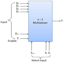
Fig 1: Block diagram of multiplexer
Multiplexers come in multiple variations
● 2: 1 multiplexer
● 4: 1 multiplexer
● 16: 1 multiplexer
● 32: 1 multiplexer
Block Diagram of 2:1 MUX
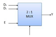
Fig 2: 2:1 MUX
Truth Table of 2:1 MUX

Where x is don’t care.
Q2) What is demultiplexer?
A2) Demultiplexer
● It performs the inverse operation of a multiplexer as it receives one input and distributes it across its outputs.
● It has only one input and n outputs with m select input.
● At a time only one output line is selected by the select lines and that input is transmitted through the output line.
● It is equivalent to a single pole multiple way switch.
Various Demultiplexers are used as:
- 1: 2 demultiplexer
- 1: 4 demultiplexer
- 1: 16 demultiplexer
- 1: 32 demultiplexer
Block diagram
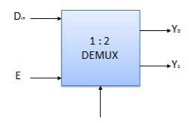
Truth Table

Where x is don’t care.
Q3) Describe decoder?
A3) Decoder
● It works as an inverse of an encoder.
● It is a combinational circuit which converts n input lines into 2n output lines.
● Taking an example of 3-to-8-line decoder.
Truth Table –
X | Y | Z | D0 | D1 | D2 | D3 | D4 | D5 | D6 | D7 |
0 | 0 | 0 | 1 | 0 | 0 | 0 | 0 | 0 | 0 | 0 |
0 | 0 | 1 | 0 | 1 | 0 | 0 | 0 | 0 | 0 | 0 |
0 | 1 | 0 | 0 | 0 | 1 | 0 | 0 | 0 | 0 | 0 |
0 | 1 | 1 | 0 | 0 | 0 | 1 | 0 | 0 | 0 | 0 |
1 | 0 | 0 | 0 | 0 | 0 | 0 | 1 | 0 | 0 | 0 |
1 | 0 | 1 | 0 | 0 | 0 | 0 | 0 | 1 | 0 | 0 |
1 | 1 | 0 | 0 | 0 | 0 | 0 | 0 | 0 | 1 | 0 |
1 | 1 | 1 | 0 | 0 | 0 | 0 | 0 | 0 | 0 | 1 |
Implementation
D0 is high when X = 0, Y = 0 and Z = 0. Hence,
D0 = X’ Y’ Z’
Similarly,
D1 = X’ Y’ Z
D2 = X’ Y Z’
D3 = X’ Y Z
D4 = X Y’ Z’
D5 = X Y’ Z
D6 = X Y Z’
D7 = X Y Z
Hence,
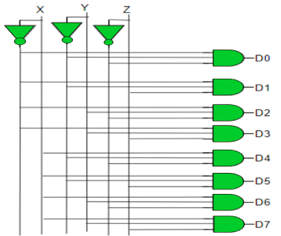
Fig 3: Decoder
Q4) Explain the encoder?
A4) Encoder
● Binary code of N digits is used to store 2N distinct elements of coded information.
● This is the reason why encoders and decoders are used.
● Encoders convert 2N lines of input into a code of N bits and Decoders decode those N bits into 2N lines.
- Encoders –
● It is a combinational circuit that converts binary information in the form of a 2N input lines into N output lines, which represent N bit code for the input.
● For simple encoders, only one input line is active at a time.
● For example: Octal to Binary encoder takes 8 input lines and generates 3 output lines.
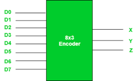
Fig 4: 8X3 Encoder (ref. 2)
Truth Table –
D7 | D6 | D5 | D4 | D3 | D2 | D1 | D0 | X | Y | Z |
0 | 0 | 0 | 0 | 0 | 0 | 0 | 1 | 0 | 0 | 0 |
0 | 0 | 0 | 0 | 0 | 0 | 1 | 0 | 0 | 0 | 1 |
0 | 0 | 0 | 0 | 0 | 1 | 0 | 0 | 0 | 1 | 0 |
0 | 0 | 0 | 0 | 1 | 0 | 0 | 0 | 0 | 1 | 1 |
0 | 0 | 0 | 1 | 0 | 0 | 0 | 0 | 1 | 0 | 0 |
0 | 0 | 1 | 0 | 0 | 0 | 0 | 0 | 1 | 0 | 1 |
0 | 1 | 0 | 0 | 0 | 0 | 0 | 0 | 1 | 1 | 0 |
1 | 0 | 0 | 0 | 0 | 0 | 0 | 0 | 1 | 1 | 1 |
● From the above truth table, it is seen that the output is 000 when D0 is active; 001 when D1 is active; 010 when D2 is active and so on.
Implementation –
● From the above truth table, the output Z is active when the input octal digit is 1, 3, 5 or 7.
● Y is active when input octal digit is 2, 3, 6 or 7 and X is active when input octal digits 4, 5, 6 or 7.
● Hence, the Boolean functions would be:
X = D4 + D5 + D6 + D7
Y = D2 +D3 + D6 + D7
Z = D1 + D3 + D5 + D7
● Hence, the encoder is realized with OR gates as follows:
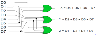
Fig 5: 8:3 encoder
● Limitation of the encoder is that only one input is active at a time.
● If more than one input is active, then the output of encoder is undefined.
● For example, if D6 and D3 are both active, then, our output would be 111 which is the output for D7.
● Problem arises when all inputs are 0.
● The encoder gives output 000 which actually is the output for D0. To avoid this, an extra bit is added to the output which is called the valid bit whose value is 0 when all inputs are 0 or 1.
Priority Encoder:
● It is an encoder whose inputs are given priorities.
● When more than one input becomes active at the same time then the input with higher priority takes precedence w.r.to the output which is generated.
● Considering a 4:2 priority encoder.
● From the truth table given below we see that when all inputs are 0, V bit is zero and outputs are not used.
● The x in the table shows the don’t care condition, i.e. it can be 0 or 1.
● Here, D3 has highest priority, therefore, when D3 is high, output has to be 11.
● D0 has the lowest priority, hence the output would be 00 only when D0 is high and all the other input lines are low.
Truth Table –
D3 | D2 | D1 | D0 | X | Y | V |
0 | 0 | 0 | 0 | x | x | 0 |
0 | 0 | 0 | 1 | 0 | 0 | 1 |
0 | 0 | 1 | x | 0 | 1 | 1 |
0 | 1 | X | x | 1 | 0 | 1 |
1 | x | X | x | 1 | 1 | 1 |
Implementation –
The condition for valid bit to be 1 is when at least one of the inputs should be high. Hence,
V = D0 + D1 + D2 + D3
For X:
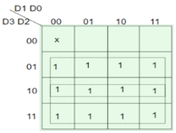
=>X=D2+D3
For Y:
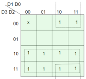
=> Y = D1 D2’ + D3
Hence, the priority 4-to-2 encoder can be realized as follows:
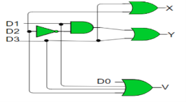
Fig 6: Priority encoder
Q5) Describe codes?
A5) Codes
● In coding, when alpha-numeric characters or words are represented by a specific group of symbols, it is said that it is being coded.
● The group of symbols is known as a code.
● The digital data can be represented, stored and transmitted as group of binary bits.
● This group is called as binary code.
● It is represented by the number as well as alphanumeric character.
Advantages of Binary Code
● They are used in computer applications.
● They are suitable for digital communications.
● They make the analysis and designing of digital circuits easy.
● Implementation becomes very easy since only 0 & 1 are being used.
Classification of binary codes
The codes are broadly classified as:
● Weighted Codes
● Non-Weighted Codes
● Binary Coded Decimal Code
● Alphanumeric Codes
● Error Detecting Codes
● Error Correcting Codes
Weighted Codes
● These codes obey the positional weight principle.
● Here each position represents a specific weight.
● Several systems are used to express the decimal digits 0 through 9.
● Here, each decimal digit is represented by a set of four bits.
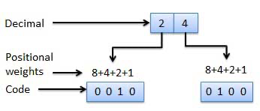
Fig 7: Weighted codes
Non-Weighted Codes
● Here, the positional weights are not assigned.
● Example: Excess-3 code and Gray code.
1.Excess-3 code
● It is also known as XS-3 code.
● It is a non-weighted code used to express decimal numbers.
● They are derived from the 8421 BCD code words adding (0011)2 or (3)10 to each code word in 8421.
● The excess-3 codes are obtained as −
Example
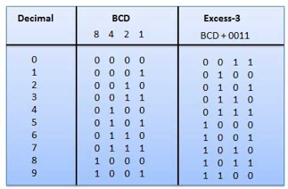
Fig 8: BCD to XS 3 conversion
2.Gray Code
● It is the non-weighted code and is not an arithmetic code.
● This means that there are no specific weights assigned to the bit position.
● Here only one bit will change every time the decimal number is incremented.
● The gray code is also known as a unit distance code as only one bit changes at a time.
● The gray code is a type of cyclic code.
● It cannot be used for all arithmetic operation.
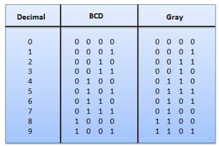
Fig 9: Gray codes (Ref. 1)
Application of Gray code
● They are used in the shaft position encoders.
● This encoder produces a code word which represents the angular position of the shaft.
3. Binary Coded Decimal (BCD) code
● Here each decimal digit is represented by a 4-bit binary number.
● Its a way to express each of the decimal digits with a binary code.
● Therefore, by four bits we can represent sixteen numbers (0000 to 1111).
● But in BCD code only first ten of these numbers are used (0000 to 1001) and rest are invalid.

Fig 10: BCD codes
Advantages of BCD Codes
● It is very similar to decimal system.
● We have to remember binary equivalent of 0 to 9 only.
Disadvantages of BCD Codes
● The addition and subtraction of BCD number system have different rules.
● The BCD arithmetic is more complicated.
● BCD code requires more number of bits than binary code to represent the decimal number.
● Hence is less efficient than binary.
4. Alphanumeric codes
➢ A binary digit or bit can be represented by two symbols as '0' or '1'.
➢ This is not sufficient for communication between two computers as we need many more symbols for communication.
➢ These symbols are represents 26 alphabetic characters with capital and small letters, numbers from 0 to 9, punctuation marks and other symbols.
➢ These alphanumeric codes represent numbers and alphabetic characters.
➢ Most of them also represent other characters like symbol and various instructions necessary for conveying information.
➢ The code at least represents 10 digits and 26 letters of alphabet i.e. total 36 items.
➢ The following three types of alphanumeric codes are commonly used for the data representation.
● American Standard Code for Information Interchange (ASCII).
● Extended Binary Coded Decimal Interchange Code (EBCDIC).
● Five bit Baudot Code.
➢ ASCII code is a 7-bit code whereas EBCDIC is an 8-bit code.
➢ ASCII code is used worldwide while EBCDIC is primarily used in large IBM computers.
5. Error Codes
➢ There technique is available to detect and correct data during data transmission.
Error Code | Description |
Error Detection and Correction | Error detection and correction code techniques |
Q6) Convert Binary to BCD?
A6) Binary to BCD Conversion
● Converting the binary number to its decimal equivalent.
● Then converting the decimal number to its equivalent BCD.
For Example –
Convert (11101)2 to BCD.
Step 1 − Convert to Decimal
Binary Number − 111012
Its Decimal Equivalent –
Step | Binary Number | Decimal Number |
Step 1 | 111002 | ((1 × 24) + (1 × 23) + (1 × 22) + (0 × 21) + (0 × 20))10 |
Step 2 | 111002 | (16 + 8 + 4 + 0 + 0)10 |
Step 3 | 111002 | 2810 |
Binary Number − 111002 = Decimal Number − 2810
Step 2 -- Convert to BCD
Decimal Number − 2810
Its BCD Equivalent:
Step | Decimal Number | Conversion |
Step 1 | 2810 | 00102 10002 |
Step 2 | 2810 | 00101000BCD |
Result
(11100)2 = (00101000)BCD
Q7) Convert BCD to Binary?
A7) BCD to Binary Conversion
● Converting the BCD number to decimal equivalent.
● Then converting decimal to binary equivalent.
For Example –
Convert (00101001)BCD to Binary.
Step 1 - Converting to BCD
BCD Number − (00101001)BCD
Its Decimal Equivalent.
Step | BCD Number | Conversion |
Step 1 | (00101001)BCD | 00102 10012 |
Step 2 | (00101001)BCD | 210 910 |
Step 3 | (00101001)BCD | 2910 |
Step 2 - BCD Number − (00101001)BCD = Decimal Number − 2910
Converting to Binary by Using long division method.
Decimal Number − 2910
Calculating Binary Equivalent –
Step | Operation | Result | Remainder |
Step 1 | 29 / 2 | 14 | 1 |
Step 2 | 14 / 2 | 7 | 0 |
Step 3 | 7 / 2 | 3 | 1 |
Step 4 | 3 / 2 | 1 | 1 |
Step 5 | 1 / 2 | 0 | 1 |
So, Decimal Number − 2910 = Binary Number − 111012
Result
(00101001)BCD = (11101)2
Q8) Convert BCD to Excess - 3?
A8) BCD to Excess-3
● Converting BCD to decimal equivalent.
● Adding (3)10 to this decimal number.
● Then converting into binary to get the required excess-3 code.
For Example –
Convert (1000)BCD to Excess-3.
Step 1 − Convert to decimal
(1000)BCD = 810
Step 2 − Add 3 to decimal
(8)10 + (3)10 = (11)10
Step 3 − Convert to Excess-3
(11)10 = (1011)2
Result
(1000)BCD = (1011)XS-3
Q9) Convert Excess-3 to BCD?
A9) Excess - 3 to BCD conversion
Subtracting (0011)2 from each 4 bit of excess-3 digit to obtain the corresponding BCD code.
For Example –
Convert (10011000)XS-3 to BCD.
Given XS-3 number = 1 0 0 1 1 0 0 0
Subtract (0011)2 = 0 0 1 1 0 0 1 1
--------------------
BCD = 0 1 1 0 0 1 0 1
Result
(10011000)XS-3 = (01100101)BCD
Q10) Explain logic gates?
A10) The basic gates are namely AND gate, OR gate & NOT gate.
AND gate
It is a digital circuit that consists of two or more inputs and a single output which is the logical AND of all those inputs. It is represented with the symbol ‘.’.
The following is the truth table of 2-input AND gate.
A | B | Y = A.B |
0 | 0 | 0 |
0 | 1 | 0 |
1 | 0 | 0 |
1 | 1 | 1 |
Here A, B are the inputs and Y is the output of two input AND gate.
If both inputs are ‘1’, then only the output, Y is ‘1’. For remaining combinations of inputs, the output, Y is ‘0’.
The figure below shows the symbol of an AND gate, which is having two inputs A, B and one output, Y.

Fig 11: AND gate (ref. 1)
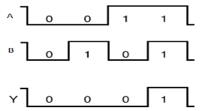
Timing Diagram:
OR gate
It is a digital circuit which has two or more inputs and a single output which is the logical OR of all those inputs. It is represented with the symbol ‘+’.
The truth table of 2-input OR gate is:
A | B | Y = A + B |
0 | 0 | 0 |
0 | 1 | 1 |
1 | 0 | 1 |
1 | 1 | 1 |
Here A, B are the inputs and Y is the output of two input OR gate.
When both inputs are ‘0’, then only the output, Y is ‘0’. For remaining combinations of inputs, the output, Y is ‘1’.
The figure below shows the symbol of an OR gate, which is having two inputs A, B and one output, Y.

Fig 12: OR gate (ref. 1)
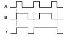
Timing Diagram:
NOT gate
It is a digital circuit that has one input and one output. Here the output is the logical inversion of input. Hence, it is also called as an inverter.
The truth table of NOT gate is:
A | Y = A’ |
0 | 1 |
1 | 0 |
Here A and Y are the corresponding input and output of NOT gate. When A is ‘0’, then, Y is ‘1’. Similarly, when, A is ‘1’, then, Y is ‘0’.
The figure below shows the symbol of NOT gate, which has one input, A and one output, Y.

Fig 13: NOT gate (ref. 1)
Timing Diagram:
Q11) Describe flip flops?
A11) Flip flops
The term "flip flop" refers to a circuit with two stable states. These stable states are used to hold binary data that can be modified by changing the inputs. The flip flops are the digital system's essential building pieces. Data storage elements include flip flops and locks. The flip flop is the simplest storage element of a sequential logical circuit. Latches and flip flops are both basic storage pieces, yet they work in distinct ways.
Types of flip flops
Flip flops come in a variety of styles:
SR flip flop
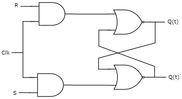
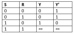
In the digital system, the S-R flip flop is the most popular flip flop. When the set input "S" is true in an SR flip flop, the output Y is high and Y' is low. When the outputs are established, it is necessary to maintain the circuit wiring. We keep the wiring in place until the set or reset input gets high or the power is turned off.
Truth table
JK flip flops
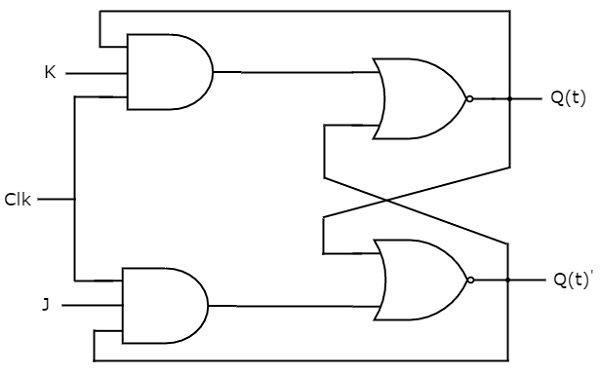
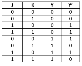
The JK flip flop is used to eliminate the S-R flip flop's problem of indeterminate states. The JK flip flop is created by making changes to the SR flip flop. In order to produce the J-K flip flop, the S-R flip flop is upgraded. The SR flip flop produces an erroneous output when both S and R inputs are set to true. In the instance of the JK flip flop, however, the output is right.
Truth table
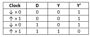
D flip flops
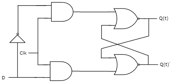
In digital systems, the D flip flop is a common flip flop. Shift registers, counters, and input synchronization all require the D flip flop.
Truth table
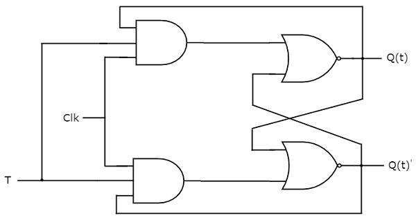
T flip flops
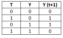
T flip flop is used in the same way that JK flip flop is. In contrast to JK flip flops, T flip flops have only one input: the clock input. The T flip flop is made by combining both of the JK flip flop's inputs into a single input.
Truth table
Q12) What is memory transfer?
A12) Memory Transfer
Most of the standard notations used for specifying operations on memory transfer are stated below.
■ The transfer of information from a memory unit to the user end is called a Read operation.
■ The transfer of new information to be stored in the memory is called a Write operation.
■ A memory word is designated by the letter M.
■ We must specify the address of memory word while writing the memory transfer operations.
■ The address register is designated by AR and the data register by DR.
Thus, a read operation can be stated as
Read: DR ← M [AR]
The Read statement causes a transfer of information into the data register (DR) from the memory word (M) selected by the address register (AR).
And the corresponding write operation can be stated as:
Write: M [AR] ← R1
The Write statement causes a transfer of information from register R1 into the memory word (M) selected by address register (AR).
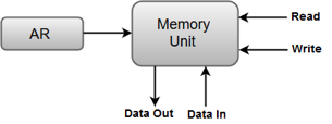
Fig 15: Showing Read and Write Operation.
Q13) Write about bus and memory transfer?
A13) Bus and Memory Transfers:
A bus consists of a set of common lines, one for each bit of register, through which binary information is transferred one at a time. Control signals determine which register is selected by the bus during a particular register transfer.
The following block diagram shows a Bus system for four registers. It is constructed with the help of four 4 * 1 Multiplexers each having four data inputs (0 through 3) and two selection inputs (S1 and S2).
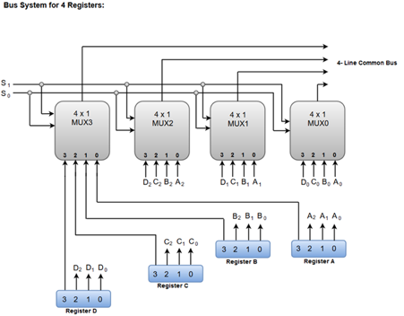
The two selection lines S1 and S2 are connected to the selection inputs of all four multiplexers. The selection lines choose the four bits of one register and transfer them into the four-line common bus.
When both of the select lines are at low logic, i.e. S1S0 = 00, the 0 data inputs of all four multiplexers are selected and applied to the outputs that forms the bus. This, in turn, causes the bus lines to receive the content of register A since the outputs of this register are connected to the 0 data inputs of the multiplexers.
Similarly, when S1S0 = 01, register B is selected, and the bus lines will receive the content provided by register B.
The following function table shows the register that is selected by the bus for each of the four possible binary values of the Selection lines.
S1 | S2 | Register Selected |
0 | 0 | A |
0 | 1 | B |
1 | 0 | C |
1 | 1 | D |
Q14) Define logic micro operation?
A14) Logic operations are binary micro-operations that are performed on bits saved in registers. These operations created binary variables by treating each bit separately.
The phrase, for example, denotes the exclusive-OR micro-operation with the values of two registers R1 and R2.
P: R1←R1 ⊕ R2
It determines a logic micro-operation to be implemented on the single bits of the registers supported by P = 1. Consider the four bits in each register. R1's content should be 1010, while R2's should be 1100.
The exclusive-OR micro-operation described above represents the logic calculation outlined below:
1010 Content of R1
1100 Content of R2
0110 Content of R1 after P = 1
Following the micro-operation, the content of R1 resembles the bit-by-bit exclusive-OR operation on pairs of bits in R2 and prior values of R1.
Special Symbols
The logic micro-operations OR, AND, and complement will be given special symbols to distinguish them from the matching symbols that can form Boolean functions. The symbol V can be used to represent an OR micro-operation, and the symbol can also be used to represent an AND micro-operation.
The complement micro-operation is similar to the 1's complement in that it supports a bar on the symbol's highest point that shows the registered name. There are several symbols that can be used to distinguish a logic micro-operation from a control (or Boolean) function.
Supporting two sets of symbols that recognize the symbol +, which can indicate arithmetic plus, from a logic OR operation has another meaning. Despite the fact that the + symbol has two meanings, it will be possible to distinguish between them by looking at where it appears.
Arithmetic plus is shown when the symbol + appears in a micro-operation. It indicates an OR operation when it appears in a control (or Boolean) function. It can't be used to represent an OR micro-operation.
For instance, consider the following statement:
P+Q: R1←R2+R3,R 4←R5V R6
An OR operation between two binary variables in a control function is the + between P and Q. An add micro-operation is determined by the + between R2 and R3. The symbol V between registers R5 and R6 denotes the OR micro-operation.
Q15) Explain shift micro operations?
A15) Shift micro-tasks are utilized for serial data transport, as well as supporting arithmetic, logic, and a variety of data-processing operations. A register's contents can be relocated to the left or right.
The first flip-flop holds its binary data from the serial input while the bits are moved. The shift-left operation moves a bit to the rightmost location on the serial input. When you shift right, the serial input moves a bit to the leftmost location. The type of shift is determined by the data sent by the serial input.
Types of shift micro operations
The following are the three categories of shift micro-operations:
1. Logical shift
It sends 0 over the serial input. The symbol "shl" denotes logical shift left, while "shr" denotes logical shift right.
R1 ←R1 shl R1
R2 ←R1 shr R2
On both sides of the arrows, the register sign should be the same.
2. Circular shift
This moves the bits of the register around the two ends without affecting the data or contents. The shift register's serial output is linked to its serial input in circular shift. The terms "cir" and "cil" stand for left and right circular shifts, respectively. The table shows the symbolic documentation for the shift micro-operations.
Shift micro operations
Symbolic Designation | Description |
R ←R1 shl R | Shift-left register R |
R ←R1 shr R | Shift-right register R |
R ←R1 cil R | Circular shift-left register R |
R ←R1 cir R | Circular shift-right register R |
R ←R1 ashl R | Arithmetic shift-left R |
R ←R1 ashr R | Arithmetic shift-right R |
3. Arithmetic shift
A signed binary number is shifted to the left or right using this method. An arithmetic shift left multiplies a signed binary number by two and divides it by two. Due to the fact that when a signed number is multiplied or divided by two, the sign bit remains constant, the arithmetic shift micro-operation leaves the sign bit constant.
Rn-1 | Rn-2 | R→ | R1 | R0 |
Sign bit
Arithmetic shift Right
The sign bit is influenced by the leftmost bit in a register, whereas the other bits influence the number. Positives have a sign bit of 0 while negatives have a sign bit of 1. Negative numbers are written in the form of 2's complement. A n-bit symbolic register is shown in the diagram.
The sign bit is held by bit Rn-1 in the leftmost position.
Rn-2 is the number's most significant digit.
The least significant bit is R0. The shift-right arithmetic keeps the sign bit constant while shifting the integer (which includes the sign bit) to the right. Therefore
Rn-1 remains the equal,
Rn-2 receives the bit from
Rn-1 and so on for the other bits in the register. The bit in
R0 is lost.
Q16) What is register transfer?
A16) The availability of hardware logic circuits that can perform a specific micro-operation and transfer the outcome of the operation to the same or another register is referred to as Register Transfer.
The majority of the standard notations for describing operations on different registers are listed here.
● MAR designates the memory address register.
● The address of the next instruction is stored in the Program Counter PC.
● The instruction being executed is stored in the Instruction Register IR.
● R1 (Processor Register).
● Individual bits can also be indicated by putting them in parenthesis. For example, PC (8-15), R2 (5), and so on.
● The replacement operator is used to represent data transfer from one register to another in symbolic form. The following sentence, for example, signifies a data transfer from register R1 to register R2.
R2 ← R1
● Most users prefer that the transfer take place only under specific control conditions. The following if-then sentence demonstrates this:
If (P=1) then (R2 ← R1); Here P is a control signal generated in the control section.
● Separating the control variables from the register transfer operation makes it easier to specify a control function (P). The following sentence, for example, specifies the data transmission operation for a certain control function (P).
P: R2 ← R1
Q17) Write about register transfer language?
A17) Register Transfer Language
Digital modules such as registers, decoders, arithmetic elements, and control logic are interconnected in a digital computer system. To make a comprehensive digital system, these digital modules are integrated with some common data and control channels. Furthermore, the registers and the actions performed on the data stored in them best describe digital modules. Micro-operations are operations that are done on data contained in registers.
The set of registers and the data flow between them are the best ways to define:
● The internal hardware organization of a digital system.
● The order in which micro-operations are done on data stored in registers.
● The control routes that start the micro-operation sequence.
The Register Transfer Language (RTL) is a symbolic representation of the notations used to define the order in which micro-operations are performed.
Data is transferred between processor registers and memory, as well as between processor registers and input-output systems, in a computer system. The following standard notations can be used to express these data transfers:
● Processor registers are denoted by the letters R0, R1, R2,..., and so on.
● Names like LOC, PLACE, MEM, and others are used to denote memory addresses.
● DATA IN, DATA OUT, and other designations are used to denote input-output registers.
● Placing square brackets around the name of the register or memory location denotes the content of the register or memory location.
Q18) How to design arithmetic logic unit?
A18) The Arithmetic Logic Unit (ALU) is the heart of any CPU. An ALU performs three kinds of operations.
● Arithmetic operations such as Addition/Subtraction,
● Logical operations such as AND, OR, etc. and
● Data movement operations such as Load and Store
ALU derives its name because it performs arithmetic and logical operations. A simple ALU design is constructed with Combinational circuits. ALUs that perform multiplication and division are designed around the circuits developed for these operations while implementing the desired algorithm. More complex ALUs are designed for executing Floating point, Decimal operations and other complex numerical operations. These are called Coprocessors and work in tandem with the main processor.
The design specifications of ALU are derived from the Instruction Set Architecture. The ALU must have the capability to execute the instructions of ISA. An instruction execution in a CPU is achieved by the movement of data/datum associated with the instruction. This movement of data is facilitated by the Datapath. For example, a LOAD instruction brings data from memory location and writes onto a GPR. The navigation of data over datapath enables the execution of LOAD instruction. We discuss Datapath more in details in the next chapter on Control Unit Design. The trade-off in ALU design is necessitated by the factors like Speed of execution, hardware cost, the width of the ALU.
Combinational ALU
A primitive ALU supporting three functions AND, OR and ADD is explained in figure below. The ALU has two inputs A and B. These inputs are fed to AND gate, OR Gate and Full ADDER. The Full Adder also has CARRY IN as an input. The combinational logic output of A and B is statically available at the output of AND, OR and Full Adder. The desired output is chosen by the Select function, which in turn is decoded from the instruction under execution. Multiplexer passes one of the inputs as output based on this select function. Select Function essentially reflects the operation to be carried out on the operands A and B. Thus A and B, A or B and A+B functions are supported by this ALU. When ALU is to be extended for more bits the logic is duplicated for as many bits and necessary cascading is done. The AND and OR logic are part of the logical unit while the adder is part of the arithmetic unit.
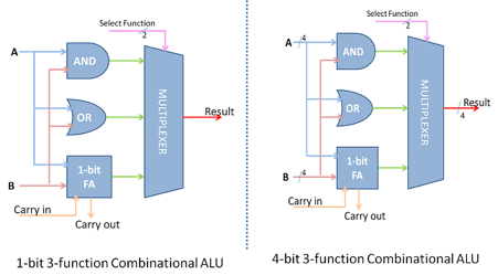
Fig 16: A Primitive ALU supporting AND, OR and ADD function
The simplest ALU has more functions that are essential to support the ISA of the CPU. Therefore the ALU combines the functions of 2's complement, Adder, Subtractor, as part of the arithmetic unit. The logical unit would generate logical functions of the form f(x,y) like AND, OR, NOT, XOR etc. Such a combination supplements most of a CPU's fixed point data processing instructions.
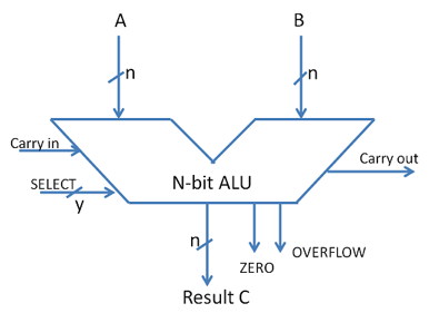
Fig 17: ALU Symbol
Q19) Write the difference between multiplexer and demultiplexer?
A19) Difference between Multiplexer and Demultiplexer
Multiplexer (MUX) | Demultiplexer (DEMUX) |
A multiplexer is a combinational circuit that provides single output but accepts multiple data inputs. | A demultiplexer is a combinational circuit that takes single input but that input can be directed through multiple outputs. |
It performs parallel to serial conversion. | It performs serial to parallel conversion. |
It has multiple inputs and one output. | It has one input and multiple outputs. |
It works on many-to-one operation principle. | It works on one-to-many operational principle. |
In time division multiplexing, multiplexer is used at the transmitter end. | In time division multiplexing, demultiplexer is used at the receiver end. |
MUX system increases the efficiency of the communication system by allowing the transmission data, such as audio and video transmission. | DEMUX receive the output signals from the multiplexer and convert them back to the original form at the receiver end. |
Q20) What are the difference between encoder and decoder?
A20) Difference between Encoder and Decoder
BASIS OF COMPARISON | ENCODER | DECODER |
Description | The encoder is basically a combinational circuit that converts the applied information signal into a coded digital bit stream. | A decoder is a circuit that changes a code into a set of signals. It is referred to as decoder because it does the reverse of encoding (recovering the original information signal from the coded bits). |
Input Signal | The applied signal is the active signal input. | Decoder accepts coded binary data as its input. |
Number Of Input | The number of inputs accepted by an encoder is 2n. | The number of input accepted by decoder is only n inputs. |
Output lines | The output lines for an encoder are n. | The output lines of a decoder are 2n. |
Operation | The operation of an encoder is quite simple. | The operation of an encoder is quite simple but the operation of the decoder is complex as it requires understanding the coding format of the encoder. |
Installation | In a communication system, the encoder circuit is installed at the transmitting end. | In a communication system, the decoder circuit is installed at the receiving side. |
Logic Element | OR gate is the basic logic element used in the encoder. | AND gate along with NOT gate is the basic logic element used in the decoder. |
Application | It is used in E-mail, video encoders etc. | It is used in microprocessors, memory chips etc. |