MP
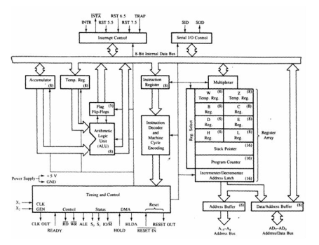
Unit-1Microprocessor evolution and typesQ1) Explain the importance of microprocessor and explain its generations?A1) The microprocessor has become a more essential part of many gadgets. The evolution of microprocessor was divided into five generations such as first, second, third, fourth, and fifth-generation and the characteristics of these generations are discussed below.First Generation MicroprocessorsThe first-generation microprocessors were introduced in the year 1971-1972. The instructions of these microprocessors were processed serially, they fetched the instruction, decoded and then executed it. When an instruction of the microprocessor was finished, then the microprocessor updates the instruction pointer & fetched the following instruction, performing this consecutive operation for each instruction in turn.Second Generation MicroprocessorsIn the year 1970, a small number of transistors were available on the integrated circuit in the second-generation microprocessors. Examples of the second-generation microprocessors are 16-bit arithmetic 7 pipelined instruction processing, MC68000 Motorola microprocessor. The second generation of the microprocessor is defined by overlapped fetch, decode, and execute the steps. When the first generation is processed in the execution unit, then the second instruction is decoded and the third instruction is fetched.Third Generation MicroprocessorsThe third generation microprocessors were introduced in the year 1978, as denoted by Intel’s 8086 and the Zilog Z8000. These were 16-bit processors with a performance like mini computers. These types of microprocessors were different from the previous generations of microprocessors in that all main workstation industrialists began evolving their own ISC based microprocessor architectures.Fourth Generation MicroprocessorsAs many industries converted from commercial microprocessors to in house designs, the fourth generation microprocessors are entered with outstanding design with a million transistors. Leading-edge microprocessors like Motorola’s 88100 and Intel’s 80960CA could issue & retire more than one instruction per clock cycle.Fifth Generation MicroprocessorsFifth-generation microprocessors employed decoupled superscalar processing, and their design soon exceeded 10 million transistors. In the fifth generation, PCs are a low-margin, high volume business conquered by a single microprocessor.Q2) Mention the types of microprocessors?A2) 4-bit MicroprocessorThe INTEL 4004/4040 was invented in the year 1971 by Stanley Mazor & Ted Hoff. The clock speed of this microprocessor is 740 KHz. 8-bit MicroprocessorThe 8008 processor was invented in the year 1972. The clock speed of this microprocessor is 500 KHz and instruction per second is 50K The 8080 microprocessor was invented in the year 1974. The clock speed is 2 MHz. The number of transistors used is 60k and instruction per second is 10 times quicker as compared with 8008 processor. The 8085 microprocessor was invented in the year 1976. The clock speed is 3 MHz. The number of transistors used is 6,500 and instruction per second is 769230. The number of pins of this microprocessor is 40 16-bit MicroprocessorThe 8086 microprocessor was invented in the year 1978. The clock speed is 4.77, 8 & 10 MHz. The number of transistors used is 29000 and instruction per second is 2.5 Million. The number of pins of this microprocessor is 40 The 8088 microprocessor was invented in the year 1979 and instruction per second is 2.5 Million The microprocessors like 80186 or 80188 were invented in the year 1982. The clock speed is 6 MHz 64-bit MicroprocessorThe INTEL core 2 microprocessor was invented in the year 2006. The clock speed is 1.2 GHz to 3 GHz. The number of transistors used is 291 Million and instruction per second is 64 KB of L1 cache for each core 4 MB of L2 cache. The i3, i5, i7 microprocessors were invented in the years 2007, 2009, 2010 2. The clock speed is 2GHz to 3.3GHz, 2.4GHz to 3.6GHz & 2.93GHz to t 3.33GHz. Q3) Explain the architecture of microprocessor?A3) It includes the timing & control unit, Arithmetic and logic unit, decoder, instruction register, interrupt control, a register array, serial input/output control and the central processing unit. Operations of 8085 MicroprocessorIt performs all arithmetical and logical operations like add, subtract, AND, OR etc. The temporary registers and accumulators hold the information throughout the operations and the result is stored in the accumulator. The different flags are arranged or rearranged on the basis of result. Flag RegistersIt is an 8 bit register. They are of five types namely sign, zero, auxiliary carry, parity and carry. Control and Timing UnitIt coordinates with all the processes of the microprocessor by the clock and provides the control signals required for communication between the microprocessor and peripherals. It is used to control the internal as well as external circuits.Decoder and Instruction Register when an order is received from memory which is located in the instruction register, it is encoded & decoded into various device cycles. Register ArrayThe general purpose registers are classified into several types such as B, C, D, E, H, & L. They are 8-bit registers. The register pairs are BC, DE & HL.Special Purpose Registers These registers are of four types namely program counter, stack pointer, increment or decrement register, address or data buffer. Program CounterIt is a 16 bit register. It is used to store data, memory information etc. whenever memory is incremented, the PC then points to the next location. Stack Pointer It is a 16 bit register. It always points to stack which can be incremented or decremented by PUSH and POP instruction. Increment or Decrement RegisterIt is an 8-bit register which can be increased or decreased by one. It is useful for incrementing or decrementing program counters as well as stack pointer register content with one. This operation can be done on any memory location or any kind of register. Address Bus and Data BusData bus carries the data required to be stored. It is bidirectional. Address bus carries the location to where the data should be stored and it is unidirectional. It is used to transfer the data & address.
Fig.1: Architecture of 8085 (ref 1)Q4) Describe the addressing modes of microprocessor?A4) The instructions are used to transfer the data from one register to another register, from the memory to the register, and from the register to the memory without any change in the content. Addressing modes in 8085 is divided into 5 groups −o Immediate addressing modeHere, the 8/16-bit data is specified in the instruction itself as one of its operand. Example: MVI B, 40F means 40F is copied into register B.o Register addressing modeHere, the data is copied from one register to another. Example: MOV B, A: means data in register A is copied to register B.o Direct addressing modeHere, the data is directly copied from the given address to the register.Example: LDB 5008H: means the data at address 5008H is copied to register B.o Indirect addressing modeHere, the data is transferred from one register to another by using the address pointed by the register. Example: MOV B, K: means data is transferred from the memory address pointed by the register K to the register B.o Implied addressing modeHere, it doesn’t require any operand; the data is specified by the opcode itself. Example: CMP.Q5) Explain data transfer scheme of microprocessor?A5)
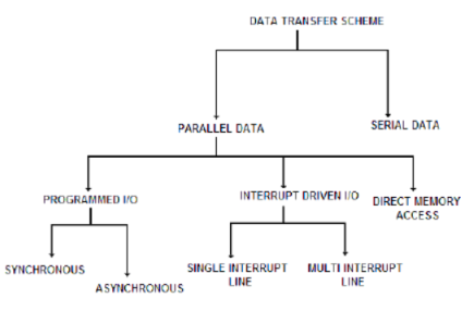
Fig.2: Data transfer schemes (Ref 3)Interruption can be done at the time of executing program by the virtue of the program by an Input Output device. It can also be done by the method as per the working of the processor. The data transfer schemes wants sending information to the processor, rather than receiving information from the processor because sending and receiving information plays a vital role for executing the entire program. The communication is not done directly with the Input Output device. It is carried out systematically with the help of Input Output device by the virtue of an Input Output port. The data transfer schemes are as follows: Serial data transfer scheme Parallel data transfer scheme Programmed I/O Data Transfer Interrupt Driven I/O data Transfer Direct memory access data transfer Q6) Explain data transfer and arithmetic instructions of microprocessor?A6)Data Transfer (copy) InstructionsThese instructions perform the following six operations:Load 8-bit number in a register.Load 16-bit number in a register pair.Copy from register to register.Copy between register and memory.Copy between I/O and accumulator.Copy between registers and stack memory.MVI R, 8-bitMOV Rd, RsLXI Rp, 16-bit OUT 8-bitIN 8-bitLDA 16-bitSTA 16-bitLDAX RpSTAX RpMOV R, MMOV M, R
|
|
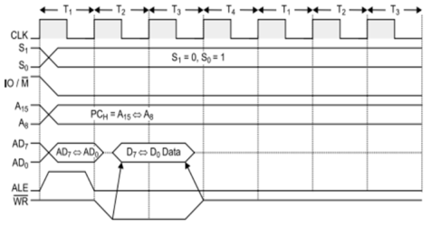
Arithmetic InstructionsThe frequently used arithmetic operations are: Add, Subtract, Increment (add 1), Decrement (subtract 1)ADD RADI 8-bitADD MSUB RSUI 8-bitSUM MINR RINR MDCR RDCR MINX RpDCX RpQ7) Draw and explain the timing diagram of memory write cycle?A7) Memory write cycle
Fig.3 Memory write Cycle

 It is used to send one byte at a time into memory. It requires 3 T-States. During T1 state, ALE = 1 and contains lower address A0-A7 from multiplexed lines AD0-AD7 and A8-A15 contains higher byte of address. As it is memory operation, IO/M = 0. During T2 state, ALE = 0, WR = 0 and address is removed from AD0-AD7 and data appears on AD0-AD7. Data remains on AD0-AD7 till WR = 0.Q8) Draw the timing diagram of I/O write cycle?A8) I/O write cycle
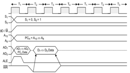
Fig.4: I/O write Cycle

 It is used to write one byte at a time into IO device. It requires 3 T-States. During T1 state, the lower byte of address is copied into higher order address bus A8-A15. ALE =1 and A0-A7 address is selected from the multiplied lines AD0-AD7. As it is an IO operation, IO/M = 1. During T2 state, ALE = 0, WR = 0 and data appears on AD0-AD7 to write data into IO device. During T3 state, data remains on AD0-AD7 till WR = 0.Q9) Explain memory and I/O interfacing devices?A9) Memory InterfacingWhen we are executing any instruction, the address of memory location or an I/O device is sent out by the microprocessor. The corresponding memory chip or I/O device is selected by a decoding circuit.I/O interfacingAs we know, keyboard and displays are used as communication channel with outside world. Therefore, it is necessary that we interface keyboard and displays with the microprocessor. This is called I/O interfacing. For this type of interfacing, we use latches and buffers for interfacing the keyboards and displays with the microprocessor. Q10) Explain timing diagram of memory read cycle?A10) Memory Read
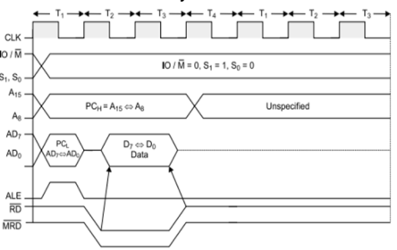
Fig.5: Memory read CycleIt fetches one byte from the memory at a time. It requires 3 T-States. It is used to fetch operand or data from the memory. During T1 state, A8-A15 contains higher byte of address, ALE is high therefore lower byte of address A0-A7 is selected from the multiplexed lines AD0-AD7.  Since it is a memory ready operation, IO/M =0.
 During T2state, ALE = 0, RD = 0 and address is removed from AD0-AD7 and data D0-D7 appears on the lines AD0-AD7.
During T3 state, data remains on AD0-AD7 till , RD = 0.
|
 It is used to send one byte at a time into memory. It requires 3 T-States. During T1 state, ALE = 1 and contains lower address A0-A7 from multiplexed lines AD0-AD7 and A8-A15 contains higher byte of address. As it is memory operation, IO/M = 0. During T2 state, ALE = 0, WR = 0 and address is removed from AD0-AD7 and data appears on AD0-AD7. Data remains on AD0-AD7 till WR = 0.Q8) Draw the timing diagram of I/O write cycle?A8) I/O write cycle
|
 It is used to write one byte at a time into IO device. It requires 3 T-States. During T1 state, the lower byte of address is copied into higher order address bus A8-A15. ALE =1 and A0-A7 address is selected from the multiplied lines AD0-AD7. As it is an IO operation, IO/M = 1. During T2 state, ALE = 0, WR = 0 and data appears on AD0-AD7 to write data into IO device. During T3 state, data remains on AD0-AD7 till WR = 0.Q9) Explain memory and I/O interfacing devices?A9) Memory InterfacingWhen we are executing any instruction, the address of memory location or an I/O device is sent out by the microprocessor. The corresponding memory chip or I/O device is selected by a decoding circuit.I/O interfacingAs we know, keyboard and displays are used as communication channel with outside world. Therefore, it is necessary that we interface keyboard and displays with the microprocessor. This is called I/O interfacing. For this type of interfacing, we use latches and buffers for interfacing the keyboards and displays with the microprocessor. Q10) Explain timing diagram of memory read cycle?A10) Memory Read
|
 Since it is a memory ready operation, IO/M =0.During T2state, ALE = 0, RD = 0 and address is removed from AD0-AD7 and data D0-D7 appears on the lines AD0-AD7.


0 matching results found