|
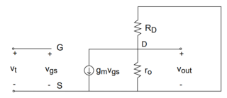
In the small signal equivalent circuit model. Remove RL and RS
Figure1. Small signal equivalent circuit model
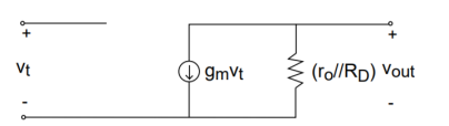
Therefore, we get
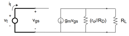
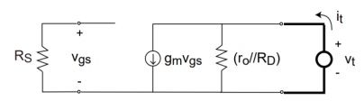
Figure2. Equivalent Small signal equivalent model vout = -gm vt (ro || RD) Then unloaded voltage gain Avo = vout / vt = -gm (ro||RD) Input resistance To calculate input resistance Apply test voltage (or current) at input and measure the test current or voltage. Rin-Load amplifier with RL Load amplifier with RL Figure3. Common source amplifier it =0 - Rin = vt/it = ∞ Output resistance: To calculate the output resistance Rout -Load amplifier with RS Measure the voltage or current at the output Set the input source equal to zero.
Figure4. CS Amplifier vgs =0 -- gm vgs =0 - vt = it(ro||RD) Rout = vt/it = ro ||RD AV = Vo / Vi = (RC/ re ) 1; AV = (RC/ re) Current gain Ai = Io / Ii Io = - Ie = - Ii Io / Ii = - -1 // check
|
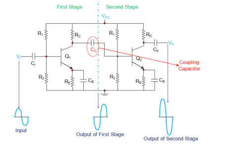
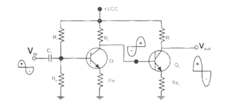
RC coupled
Figure 5. RC coupled Amplifier
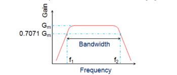
The AC component of this signal is coupled to second stage of the RC coupled amplifier through coupling capacitor CC and thus appears as an input at the base of the second transistor Q2. This is amplified further and passed-on as output of the second stage which is available at the collector terminal of Q2 after getting shift by 180o in its phase. This means that the output of the second stage will be 360o out-of-phase with respect to the input, which in turn indicates that the phase of the input signal and the phase of the output signal obtained at stage II will be identical. The frequency response of a RC coupled amplifier shown by Figure 2, indicates that the gain of the amplifier is constant over a wide range of mid-frequencies while it decreases considerably both at low and high frequencies.
Figure 6. Frequency Response of RC Coupled Amplifier
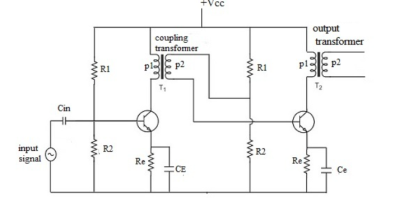
Figure 7. Transformer Coupled
In the circuit diagram, one stage output is connected as an input to the second stage amplifier through a coupling transformer. In the RC coupling amplifier, cascading of the first & second stage amplifier is done through coupling capacitor. The coupling transformer T1 & it is primary and secondary windings are P1 and P2. Similarly, secondary transformer T2 having the primary windings p1 and secondary windings are indicated by p2.
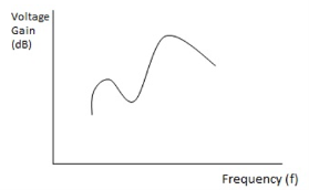
Here, the input signal is applied to the base of the first transistor. If the input signal has any DC signal, then the components can be eliminated by the input capacitor Cin. When the signal is applied to the transistor it amplifies & forwards to collector terminal. Hence the amplified output is connected as an input to the second stage of the transformer-coupled amplifier through secondary windings (p2) of the coupling transformer. This amplified voltage is applied to the base terminal of the second transistor of the secondary stage of the transformer-coupled amplifier. Frequency Response of Transformer Coupled Amplifier Figure 8. Frequency Reponse
The transformer-coupled amplifier offers constant gain over a small range of frequencies. At low frequencies, due to the reactance of the primary transformer p1, the gain is decreased. At higher frequencies, the capacitance between the turns of the transformer will act as a condenser and this reduces the output voltage, and this leads to decrement in gain. Direct Coupled Amplifier
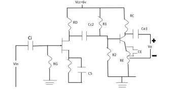
Figure 9. Direct Coupled Amplifier When +ve half cycle is applied at the input Q1 transistor biased through the divider bias network. The positive half cycle forward biases the transistor Q1 which starts conduction and provides an inverted and amplified output at the collector. We know that VCE = VCC – Ic Rc The amplified negative signal is provided as base to transistor Q2 which is self bias. The base of Q2 transistor is reverse and does not conduct , the output of Q2 is the amplified signal when Q2 does not conduct and the voltage drop across collector emitter will be zero. Therefore Vcc=IcRc Design of RC coupled amplifer Given data: Av Step 1: Circuit Diagram of amplifier circuit As the input resistance or impedance is large in given data Ri
Vcc=6V Step 2: Voltage gain calculations FET has low voltage gain Av1=10------- First stage Av2 = 150 -----Second Stage AVT = Av1 x Av2 = 10 x 150 = 1500. We first design second stage Using hybrid h-parameter Step3: Calculation of collector resistor Rc and selection of transistor. Since transistor is not specified we take BCS 47A Av2 = - hfe (Rc||RL) / hie RL =∞ Av2 = -hfe(Rc)/hie Rc = Av2.hie /hfe(min) From the data sheet hie =2.7 k hfe = 125 Rc2 = 150 x 2.7k/125 =3.24 kΩ Hence the approximate value of Rc = 3.6kΩ Step3: Calculation of Q point Vcc is given as 6V Take VCEQ as 50% Vcc to have Q point at the centre and accommodate full swing of output voltage. Take VRE as 20% Vcc VceQ = ½ Vcc = 1.2 x 6 = 3V Vre = 20% Vcc = 1.2 V Apply KVL to output loop Vcc – VRC – VCEQ -VRE =0 VRC = Vcc – VceQ – Vre = 6-3-1.2 Vrc = 1.8V We know that VRC = Ic Rc Ic = VRC/Rc = 4.6 /3.6 kΩ IcQ = 0.5 mA Q point(3V,0.5mA) Step4: Calculation of RE(emitter resistance ) Vre = IE . RE IE = (1+β) IB IB = Ic/β IB = 0.5mA/180 IB = 2.7 μA IE = (1+β) IB IE = 0.48mA RE = VRE/IE = 1.2 / 0.48mA = 2.5kΩ Select RE = 2.4 kΩ Step 5: Calculation of R1 and R2 for second stage Given Sico VB = VBE + VRE = 0.7 + 1.2 = 1.9 V But VB = Vcc.R2/ (R1+R2) VB/Vcc = R2/R1+R2 Using Thevenin’s theorem Rth = R1R2/ (R1+R2) Rth/R1 = R2/(R1+R2) For voltage divider bias stability factor is given by S S =8 hfe(max) for BC 547-A hfe max =260. Substituting in the above formula we get 8 = 1+260/ 1+260 (Rth / Rth +RE) 8/ 261 = 1/1+260(RE /Rth + RE) 261/8 = 1/1+260 (RE/Rth + RE) 32.62 = 1+260(RE/Rth+Re) 31.62 = 260(RE/Rth+RE) 0.122 = RE/Rth+RE 0.122 Rth + 0.122 RE = RE Solving for Rth we get Rth = 17.27 kΩ By using eq(1) and eq(2) we get VB/Vcc = Rth/R1 R1 = Rth x Vcc/VB = 17.27 x 10 3 x 6/ 1.9 R1=54.53 kΩ Select the higher standard value of R1 = 56kΩ. Rth = R1R2/R1+R2 17.27 x 10 3 = 56kΩ R2 / 56kΩ+ R2 R2= 24.97 kΩ Solving for R2 we get R2=24.97kΩ Therefore R2 =22kΩ Design of RC coupled amplifier with feedback Feedback reduces the overall gain of a system with the degree of reduction being related to the systems open-loop gain. Negative feedback also has effects of reducing distortion, noise, sensitivity to external changes as well as improving system bandwidth and input and output impedances.
Direct Coupled Amplifier
The design of a single stage RC coupled amplifier is shown below. Design of Re and Ce:
The remaining 50% will drop across the collector-emitter . From (1) and (2) Rc =0.4 (Vcc/Ic) and Re = 01(Vcc/Ic). Design of R1 and R2: Base current Ib = Ic/hfe. Since VR1 ,VR2 and IR1 are found we can find R1 and R2 using the following equations.
Finding Ce: Impedance of emitter by-pass capacitor should be one by tenth of Re. XCe = 1/10 (Re) XCe = 1/2πFCe
Finding Cin: Impedance of the input capacitor(Cin) should be one by tenth of the transistors input impedance (Rin). i.e. XCin = 1/10 (Rin) Rin = R1 parallel R2 parallel (1 + (hfe re)) re = 25mV/Ie. Xcin = 1/2πFCin. From this Cin can be found.
Finding Cout: Impedance of the output capacitor (Cout) must be one by tenth of the circuit’s output resistance (Rout). XCout = 1/10 (Rout). Rout = Rc. XCout = 1/ 2∏FCout. From this Cout can be found.
Setting the gain: Introducing a suitable load resistor RL across the transistor’s collector and ground will set the gain. Expression for the voltage gain (Av) of a common emitter transistor amplifier is as follows. Av = -(rc/re) re = 25mV/Ie and rc = Rc parallel RL From this RL can be found |


References:
- Fundamentals of Analog Circuits (English, Paperback, Floyd Thomas L.)
3. Analog Electronics by J.B Gupta
4. Design with Operational Amplifier and Analog Integrated Circuits by Sergio Franco.


