Unit 3
Voltage Regulator
A linear regulator operates by using a voltage-controlled current source to force a fixed voltage to appear at the regulator output terminal.
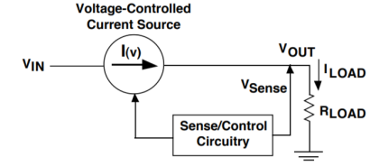
The control circuitry must monitor (sense) the output voltage, and adjust the current source (as required by the load) to hold the output voltage at the desired value.
The design limit of the current source defines the maximum load current the regulator can source and still maintain regulation.
The output voltage is controlled using a feedback loop, which requires some type of compensation to assure loop stability.
Most linear regulators have built-in compensation, and are completely stable without external components.
Some regulators (like Low-Dropout types), do require some external capacitance connected from the output lead to ground to assure regulator stability.
Another characteristic of any linear regulator is that it requires a finite amount of time to "correct" the output voltage after a change in load current demand.
This "time lag" defines the characteristic called transient response, which is a measure of how fast the regulator returns to steady-state conditions after a load change.
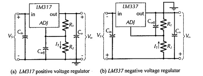
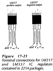
The LM317 and LM337 IC Linear Voltage Regulators are three-terminal devices which are extremely easy to use. The 317 is a positive voltage regulator [Fig. 17-24(a)], and the 337 is a negative voltage regulator [Fig. 17-24(b)]. In each case, input and output terminals are provided for supply and regulated output voltage, and an adjustment terminal (ADJ) is included for output voltage selection. The output voltage range is 1.2 V to 37 V, and the maximum load current ranges from 300 mA to 2 A, depending on the device package type. Typical line and load regulations are specified as 0.01%/(volt of Vo), and 0 3%/(volt of Vo), respectively.
The internal reference voltage for the 317 and 337 regulators is typically 1.25 V, and Vref appears across the ADJ and output terminals. Consequently, the regulator output voltage is,
Vo = R1 + R2 / R1 x Vref -------------------------(1)
To determine suitable values for R1 and R2 for a desired output voltage, first select the voltage divider current (I1) to be much larger than the current that flows in the ADJ terminal of the device. This is specified as 100 μA maximum on the device data sheet. The resistors are calculated using the relationship in Eq.
Note the capacitors included in the IC Linear Voltage Regulators circuits. Capacitor Cin is necessary only when the regulator is not located close to the power supply filter circuit. Cin eliminates the oscillatory tendencies that can occur with long connecting leads between the filter and regulator. Capacitor Co improves the transient response of the regulator and ensures ac stability, and Cadj improves the ripple rejection ratio.
Features:
The LM137 and LM337-N are adjustable 3-terminal
• 1.5-A Output Current
• Line Regulation 0.01%/V (Typical)
• Load Regulation 0.3% (Typical)
• 77-dB Ripple Rejection resistors to set the output voltage and one output capacitor for frequency compensation. The circuit
• 50 ppm/°C Temperature Coefficient
• Thermal Overload Protection.
• Internal Short-Circuit Current Limiting Protections
Specifications:
Absolute Maximum Ratings
ESD Ratings
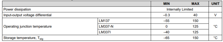
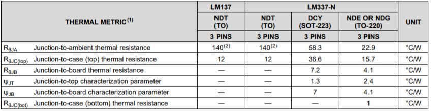
Thermal information

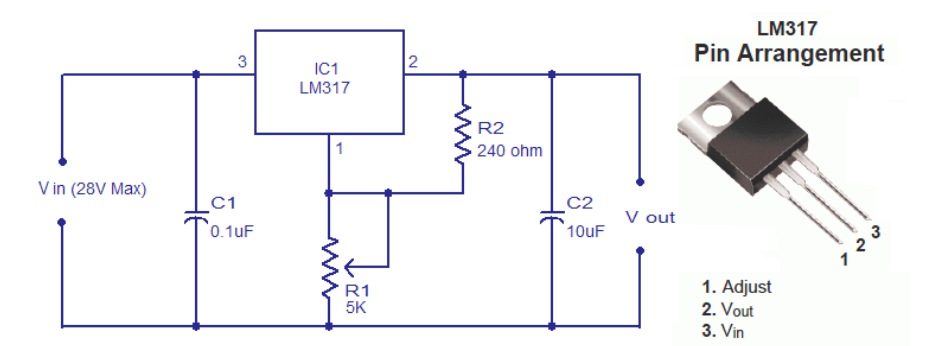
LM317 is a three terminal voltage regulator IC from National Semiconductors. The IC is capable of delivering up to 1A of output current. Input voltage can be up to 40V and output voltage can be adjusted from 1.2V to 37V.
Typical positive voltage regulator circuit using LM317.
Vout = 1.25 V (1+(R2/R1)) + (1 adj x R2 )
A classic voltage regulator circuit using LM317 is shown above. Input voltage is fed to the pin3 (v in) of the IC and regulated output voltage is available from pin 2 ( V out) of the IC.
Resistor network comprising of R1 and R2 connected in association to the pin1 (adj) is used to set the output voltage. C1 is the input filter capacitor while C2 is the output filter capacitor.
The output voltage of the regulator circuit depends on the equation,
Vout = 1.25V (1 + (R2/R1)) + I adj R2.
Volt regulators such as the LM708, and LM317 series (and others) sometimes need to provide a little bit more current then they actually can handle.
The power transistor is used to boost the extra needed current above the maximum allowable current provided via the regulator.
Current up to 1500mA(1.5amp) will flow through the regulator, anything above that makes the regulator conduct and adding the extra needed current to the output load. It is no problem stacking power transistors for even more current. Both regulator and power transistor must be mounted on an adequate heatsink.
Circuit diagram:
Voltage regulators are used to provide a stable power supply voltage independent of load impedance, input-voltage variations, temperature, and time.
Low-dropout regulators are distinguished by their ability to maintain regulation with small differences between supply voltage and load voltage.
For example, as a lithium-ion battery drops from 4.2 V (fully charged) to 2.7 V (almost discharged), an LDO can maintain a constant 2.5 V at the load.
The increasing number of portable applications has thus led designers to consider LDOs to maintain the required system voltage independently of the state of battery charge.
But portable systems are not the only kind of application that might benefit from LDOs. Any equipment that needs constant and stable voltage, while minimizing the upstream supply (or working with wide fluctuations in upstream supply), is a candidate for LDOs. Typical examples include circuitry with digital and RF loads.
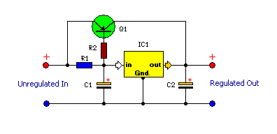
A “linear” series voltage regulator (Figure 1) typically consists of a reference voltage, a means of scaling the output voltage and comparing it to the reference, a feedback amplifier, and a series pass transistor (bipolar or FET), whose voltage drop is controlled by the amplifier to maintain the output at the required value.
If, for example, the load current decreases, causing the output to rise incrementally, the error voltage will increase, the amplifier output will rise, the voltage across the pass transistor will increase, and the output will return to its original value.
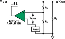 Figure 1. Basic enhancement-mode PMOS LDO.
In Figure 1, the error amplifier and PMOS transistor form a voltage-controlled current source. The output voltage, VOUT, is scaled down by the voltage divider (R1, R2) and compared to the reference voltage (VREF). The error amplifier's output controls an enhancement-mode PMOS transistor.
The dropout voltage is the difference between the output voltage and the input voltage at which the circuit quits regulation with further reductions in input voltage.
It is usually considered to be reached when the output voltage has dropped to 100 mV below the nominal value. This key factor, which characterizes the regulator, depends on load current and junction temperature of the pass transistor.
The working of SMPS is simply understood by knowing that the transistor used in LPS is used to control the voltage drop while the transistor in SMPS is used as a controlled switch.
Working
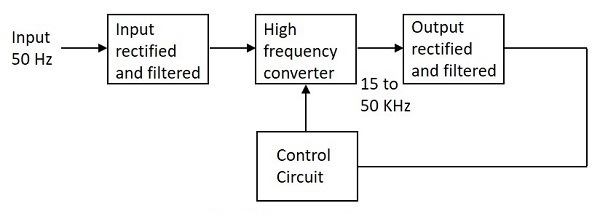
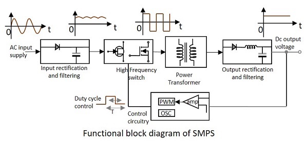
The working of SMPS can be understood by the following figure.

Input Stage
The AC input supply signal 50 Hz is given directly to the rectifier and filter circuit combination without using any transformer. This output will have many variations and the capacitance value of the capacitor should be higher to handle the input fluctuations. This unregulated dc is given to the central switching section of SMPS.
Switching Section
A fast switching device such as a Power transistor or a MOSFET is employed in this section, which switches ON and OFF according to the variations and this output is given to the primary of the transformer present in this section. The transformer used here are much smaller and lighter ones unlike the ones used for 60 Hz supply. These are much efficient and hence the power conversion ratio is higher.
Output Stage
The output signal from the switching section is again rectified and filtered, to get the required DC voltage. This is a regulated output voltage which is then given to the control circuit, which is a feedback circuit. The final output is obtained after considering the feedback signal.
Control Unit
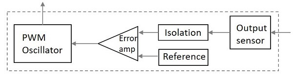
This unit is the feedback circuit which has many sections. Let us have a clear understanding about this from The following figure.

The above figure explains the inner parts of a control unit. The output sensor senses the signal and joins it to the control unit.
The signal is isolated from the other section so that any sudden spikes should not affect the circuitry. A reference voltage is given as one input along with the signal to the error amplifier which is a comparator that compares the signal with the required signal level.
By controlling the chopping frequency the final voltage level is maintained. This is controlled by comparing the inputs given to the error amplifier, whose output helps to decide whether to increase or decrease the chopping frequency. The PWM oscillator produces a standard PWM wave fixed frequency.
We can get a better idea on the complete functioning of SMPS by having a look at the following figure.

The SMPS is mostly used where switching of voltages is not at all a problem and where efficiency of the system really matters.
There are few points which are to be noted regarding SMPS. They are
Disadvantages
There are few disadvantages in SMPS, such as
Advantages
The advantages of SMPS include,
Working
The working of SMPS can be understood by the following figure.
Input Stage
The AC input supply signal 50 Hz is given directly to the rectifier and filter circuit combination without using any transformer. This output will have many variations and the capacitance value of the capacitor should be higher to handle the input fluctuations. This unregulated dc is given to the central switching section of SMPS.
Switching Section
A fast switching device such as a Power transistor or a MOSFET is employed in this section, which switches ON and OFF according to the variations and this output is given to the primary of the transformer present in this section. The transformer used here are much smaller and lighter ones unlike the ones used for 60 Hz supply. These are much efficient and hence the power conversion ratio is higher.
Output Stage
The output signal from the switching section is again rectified and filtered, to get the required DC voltage. This is a regulated output voltage which is then given to the control circuit, which is a feedback circuit. The final output is obtained after considering the feedback signal.
Control Unit
This unit is the feedback circuit which has many sections. Let us have a clear understanding about this from The following figure.
The above figure explains the inner parts of a control unit. The output sensor senses the signal and joins it to the control unit.
The signal is isolated from the other section so that any sudden spikes should not affect the circuitry. A reference voltage is given as one input along with the signal to the error amplifier which is a comparator that compares the signal with the required signal level.
By controlling the chopping frequency the final voltage level is maintained. This is controlled by comparing the inputs given to the error amplifier, whose output helps to decide whether to increase or decrease the chopping frequency. The PWM oscillator produces a standard PWM wave fixed frequency.
We can get a better idea on the complete functioning of SMPS by having a look at the following figure.
The SMPS is mostly used where switching of voltages is not at all a problem and where efficiency of the system really matters.
There are few points which are to be noted regarding SMPS. They are
Disadvantages
There are few disadvantages in SMPS, such as
Advantages
The advantages of SMPS include,
The different types of SMPS include the following
The main power received from the AC main is resolved and filtered as high voltage DC. Then, it is changing at an enormous rate of speed and fed to the main side of the step-down transformer. This transformer is only a segment of the size of an equivalent 50 Hz unit, thus releasing the size and weight problems. The filtered and rectified o/p at the minor side of the transformer. Then it is now sent to the o/p of the power supply. A sample of this o/p is sent back to the button to control the o/p voltage.
Forward Converter
In a forward converter, the choke transmits the current when the transistor is leading as well as when it is not. The diode transmits the current through the OFF period of the transistor. Thus, the flow of current into the load during both the periods. The choke stores energy during the ON period and also permits some energy into the o/p load.
Flyback Converter
In this converter, the magnetic field of the inductor supplies the energy throughout the ON period of the switch. The energy is collapsed into the o/p voltage circuit when the button is in the open state. The duty cycle controls the output voltage.
Self-Oscillating Flyback Converter
This is the most simple converter based on the principle of the flyback. Throughout the conduction time of the switching transistor, the flow of current through the transformer primary switches ramping up linearly with the angle equal to Vin/Lp. The induced voltage in the secondary winding and the feedback winding make the fastest recovery rectifier reverse biased and hold the conducting transistor ON.
When the primary current touches a peak value ‘Ip’, where the core activates to saturate, the current inclines to increase very sharply. This cannot be supported by the fixed base drive offered by the feedback winding. As a result, the switching activates to come out of saturation.
Features:
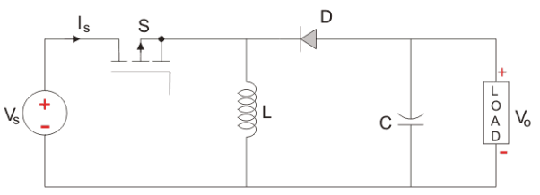
The input voltage source is connected to a solid state device. The second switch used is a diode . The diode is connected, in reverse to the direction of power flow from source, to a capacitor and the load and the two are connected in parallel as shown in the figure above.
The controlled switch is turned on and off by using Pulse Width Modulation(PWM).
PWM can be time based or frequency based. Frequency based modulation has disadvantages like a wide range of frequencies to achieve the desired control of the switch which in turn will give the desired output voltage.
Time based Modulation is mostly used for DC – DC converters . It is simple to construct and use. The frequency remains constant in this type of PWM modulation.
The Buck Boost converter has two modes of operation. The first mode is when the switch is on and conducting.
Mode I : Switch is ON, Diode is OFF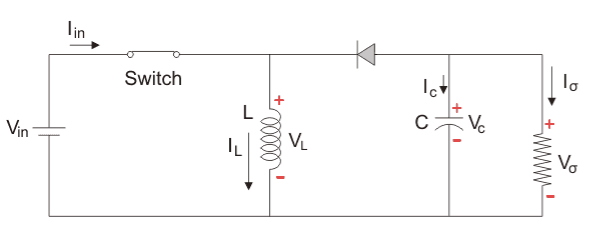
The Switch is ON and therefore represents a short circuit ideally offering zero resistance to the flow of current so when the switch is ON all the current will flow through the switch and the inductor and back to the DC input source.
The inductor stores charge during the time the switch is ON and when the solid state switch is OFF the polarity of the Inductor reverses so that current flows through the load and through the diode and back to the inductor.
So, the direction of current through the inductor remains the same.
Let us say the switch is on for a time TON and is off for a time TOFF. We define the time period, T, as T = TON + TOFFand the switching frequency,
fswitching = 1/T
Let us now define another term, the duty cycle, D = TON /T
Let us analyse the Buck Boost converter in steady state operation for this mode using KVL
Vin = VL
VL = L diL/dt = Vin
diL /dt = ∆ iL / ∆ t = ∆ iL / DT = Vin /L
Since the switch is closed for a time TON = DT we can say that Δt = DT.
(∆ iL) closed = (Vin/L ) DT
While performing the analysis of the Buck-Boost converter we have to keep in mind that
Mode II : Switch is OFF, Diode is ON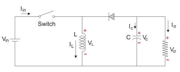
In this mode the polarity of the inductor is reversed and the energy stored in the inductor is released and is ultimately dissipated in the load resistance and this helps to maintain the flow of current in the same direction through the load and also step-up the output voltage as the inductor is now also acting as a source in conjunction with the input source.
But for analysis we keep the original conventions to analyse the circuit using KVL.
Let us now analyse the Buck Boost converter in steady state operation for Mode II using KVL
VL = Vo
VL = L diL/dt = Vo
diL /dt = ∆ iL/∆t = ∆ iL/ (1-D) T = Vo/L
Since the switch is open for a time
TOFF = T – TON = T -DT = (1-D) T we can say that ∆t = (1-D) T
It is already established that the net change of the inductor current over any one complete cycle is zero.
Since (∆ iL) closed + (∆ iL)open =0
(Vo/L) (1-D) T + (Vin/L) DT =0
Vo /Vin = -D/1-D
We know that D varies between 0 and 1. If D > 0.5, the output voltage is larger than the input; and if D < 0.5, the output is smaller than the input. But if D = 0.5 the output voltage is equal to the input voltage .
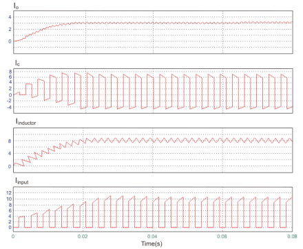
A circuit of a Buck-Boost converter and its waveforms is shown below.
The inductance L, is 50mH and the C is 100µF and the resistive load is 50Ω. The switching frequency is 1 kHz. The input voltage is 100 V DC and the duty cycle is 0.5.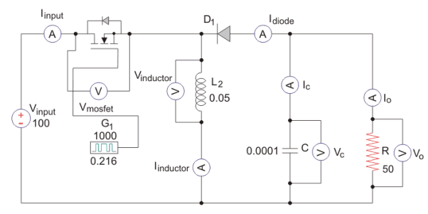
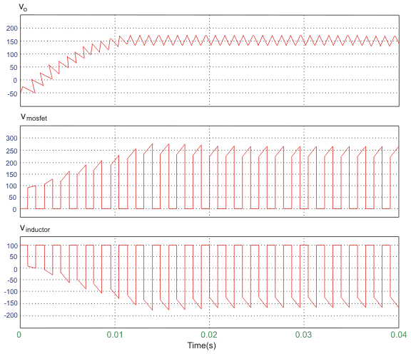
The voltage waveforms are as shown above and the current waveforms are as
Shown in the figure below.
References :
MOSFET theory and design Book by R. Warner
Operational Amplifiers - Theory and Design Book by Johan H. Huijsing
Fundamentals of Electronics: Book 2: Amplifiers: Analysis and Design Book by Ernest M. Kim and Thomas Schubert


