VLSI
UNIT - 6Testability 6.1 Types of FaultThe various fault types are:Assertion Fault. Behavioral Fault. Branch Fault. Bridging (*) Bus Fault. Cross-point Fault. Defect-oriented Fault (physical level faults, bridging, stuck-open, IDDQ). 6.2 Need of Design for Testability (DFT)DFT is a technique, which facilitates a design to become testable after fabrication. Add on logic is added along with the design logic during implementation process helps in post-production testing. Post-production testing is necessary because, the process of manufacturing is not 100% error free. There are defects in silicon which contribute towards the errors introduced in the physical device. A chip will not work as per the specifications if there are any errors introduced in fabrication. All the functional tests run on each of a million physical devices, is very time consuming, there was a need for a method, which assures it's maturity without running full exhaustive tests on the physical device in order to ensure that the device has been manufactured correctly. 6.3 TestabilityThe increasing capability of fabricating a very large number of transistors on a single integrated-circuit chip and the complexity of the possible systems has increased the importance of being able to test such circuits in an acceptable way and in an acceptable time. The time difficulties of tests are primarily due to the limited number of I/O. The connections on a chip is the only means of access to the circuit, the ratio of the number of gates on a chip to the number of accessible I/Os goes on increasing with chip size. To minimize the difficulties, present methods are adopted to make the problem manageable. This involves a consideration of the testability of the circuit at the design stage, with some partitioning and structured design methodology essential in the case of very complex circuits. 6.4 Fault ModelsA fault model is an engineering model that could go wrong in the construction or operation of a piece of equipment. From the model, the designer or user can then predict the consequences of this particular fault. Fault models can be used in almost all branches of engineering.Basic fault models in digital circuits include:Static faults, which give incorrect values at any speed and sensitized by performing only one operation: In this, a signal, or gate output, is stuck at a 0 or 1 value, independent of the inputs to the circuit.The bridging fault model. Here, two signals are connected together when they should not be. Depending on the logic circuitry employed, this may result in a wired-OR or wired-AND logic function. Since there are O(n2) potential bridging faults, they are normally restricted to signals that are physically adjacent in the design.The transistor faults. This model describes faults for CMOS logic gates. At transistor level, a transistor maybe stuck-short or stuck-open. In stuck-short, a transistor behaves as it is always conducts (or stuck-on), and stuck-open is when a transistor never conducts current (or stuck-off). Stuck-short will produce a short between VDD and VSS.The open fault model. Here a wire is assumed broken, and one or more inputs are disconnected from the output that should drive them. As with bridging faults, the resulting behavior depends on the circuit implementation.Dynamic faults, only at-speed and are sensitized by performing multiple operations sequentially: 6.5 Path SensitizingThe basic principle of the path sensitization method is to choose some path from the origin of the fault to the circuit output. A path is sensitized if the inputs to the gates along the path are assigned values such that the effect of the fault can be propagated to the output.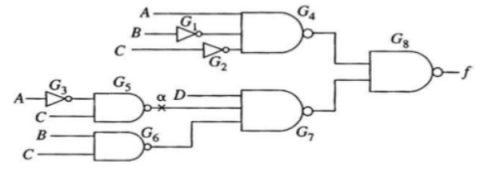 From the above fig. Assume that the line α is s-a-1.Hence to test for α, both G3 = C = 1. Also D = G6 =1 so that G7 =1 if the fault is absent. To propagate the fault from G7 to output f via G8 requires G4 = 1.This is because if G4 = 0 then output f will be forced to be 1.The process of propagating the effect of the fault from its original location to the circuit output is known as forward trace.Similar is the process of backward trace. 6.6 Sequential Circuit Test
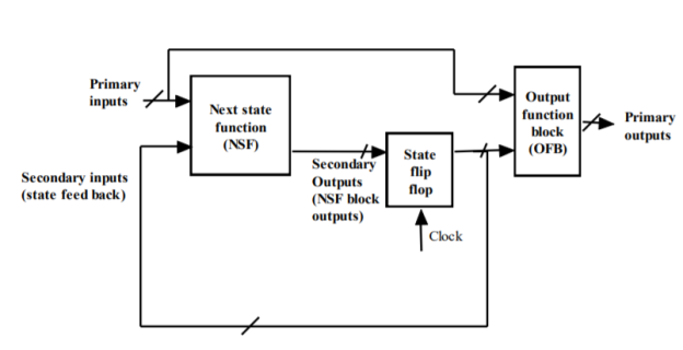 ATPG for sequential circuits. •variations required in fault model, algebra and ATPG procedure •compare the ATPG Complexity •A special scheme called “scan chain” which modifies a sequential circuit into a virtual combinational one”. When a circuit powers up, the flip-flops can have any value (0 or 1). •ATPG need to control (indirectly) the outputs of flip-flops and observe (indirectly) the inputs to the flip-flops. •Once achieved, ATPG for these combinational blocks can be done using D algorithm.•Single clock sequential circuits. •Each flip-flop is treated as 1-bit memory element with ONE common clock. •After a clock edge, the secondary output pattern (next state) is transferred to the output of the flip-flops (present state), which become new secondary inputs. Also, the primary outputs are updated. This activity occurs at each clock edge, and so it is called “synchronous” operation. •Single stuck at faults are assumed in NSF and OFB. •Internal faults of flip-flops are not modeled; their output and input faults are modeled as faults on input and output signals of the combinational blocks. •No faults are considered in the clock signal. •Most of the time, D-flip-flops are used in VLSI designs. So in this course whenever we refer to a flip-flop we essentially mean a D-flipflop. 6.7 BISTAs the complexity of VLSI circuits increases, test generation and application becomes an expensive and not always very effective means of testing. Built-in Self Test (BIST) is another solution. It is a mechanism that permits a machine to test itself. Engineers design BISTs to meet requirements such as:
high reliability lower repair cycle times or constraints such as:limited technician accessibility cost of testing during manufacture The main purpose of BIST is to reduce the complexity, and thereby decrease the cost and reduce reliance upon external (pattern-programmed) test equipment. It reduces cost in two ways: reduces test-cycle duration reduces the complexity of the test/probe setup, by reducing the number of I/O signals that must be driven/examined under tester control. Figure below shows the Built-in Self Test system.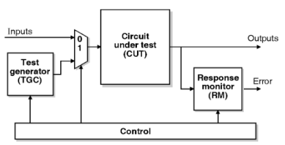 Advantages :
Lower cost due to elimination of external tester In-system, at-system, high-quality testing Faster fault detection, ease of diagnosis Overcomes pin limitations and related interfacing problems Reduces maintenance and repair costs at system level. 6.8 Test Pattern GenerationATPG (acronym for both Automatic Test Pattern Generation and Automatic Test Pattern Generator) is an electronic design automation method/technology used to find an input (or test) sequence that, when applied to a digital circuit, enables automatic test equipment to distinguish between the correct circuit behaviour and the faulty circuit behaviour caused by defects. The generated patterns are used to test semiconductor devices after manufacture, or to assist with determining the cause of failureDifferent ATPG algorithms are:Early test generation algorithms such as boolean difference and literal proposition were not practical to implement on a computer. The D Algorithm was the first practical test generation algorithm in terms of memory requirements. The D Algorithm continues to be the most used ATPG algorithms. D Algorithm tries to propagate the stuck at fault value denoted by D (for SA0) or D (for SA1) to a primary output. Path-Oriented Decision Making (PODEM) is an improvement over the D Algorithm. It became evident when design innovations resulted in circuits that D Algorithm could not realize. Fan-Out Oriented (FAN Algorithm) is an improvement over PODEM. It limits the ATPG search space to reduce computation time and accelerates back tracing. Methods based on Boolean satisfiability are sometimes used to generate test vectors. Pseudorandom test generation is the simplest method of creating tests. It uses a pseudorandom number generator to generate test vectors, and relies on logic simulation to compute good machine results, and fault simulation to calculate the fault coverage of the generated vectors. Wavelet Automatic Spectral Pattern Generator (WASP) is an improvement over spectral algorithms for sequential ATPG. It uses wavelet heuristics to search space to reduce computation time and accelerate the compactor. 6.9 JTAG & Boundary ScanThe JTAG, boundary scan test technique uses a shift register latch cell built into each external connection of every boundary scan compatible device. One boundary scan cell is included in the integrated circuit line adjacent to each I/O pin, and when used in the shift register mode it can transfer data along to the next cell in the device. There are defined entry and exit points for the data to enter and exit the device, and it is therefore possible to chain several devices together. 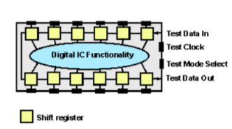 Under normal operating conditions the cell is set so that it has no effect and it becomes invisible. However when the device is set to test mode, it permits a serial data stream (test vector) to be passed from one shift register latch cell to the next. Boundary-scan cells in a device can capture data from integrated circuit line, or force data onto them. In this way a test system that can input a data stream to the shift register chain can set up states on the board, and also monitor data. By setting up one serial data stream, latching this into place, and then monitor the returning data stream, it is possible to gain access to the circuits on the board and check that a returning data stream is what is expected. If it is, then the test can pass, but if not the boundary scan system has detected and problem that can be further investigated.JTAG InterfaceThere are a number of JTAG control and data lines that form the test access port, TAP. These lines known as TCK, TMS and the optional TRST line are connected in parallel to the chips in the boundary scan chain. Connections designated TDI (input) and TDO (output) are daisy chained together to provide a path around the boundary scan chips for the data. Data is sent into the TDI of the first chip, and then TDO from the first chip is connected to TDI of the next and so forth. Finally the data is taken from the TDO of the last IC in the daisy chain.
TAP, Test Access Port - The pins associated with the test access controller. TCK, Test Clock - this pin is the clock signal used for ensuring the timing of the boundary scan system. The TDI shifts values into the appropriate register on the rising edge of TCK. The selected register contents shift out onto TDO on the falling edge of TCK. TDI, Test Data Input - Test instructions shift into the device through this pin. TDO, Test Data Output - This pin provides data from the boundary scan registers, i.e. test data shifts out on this pin. TMS, Test Mode Select - This input which also clocks through on the rising edge of TCK determines the state of the TAP controller. TRST, Test Reset - This is an optional active low test reset pin. It permits asynchronous TAP controller initialization without affecting other device or system logic. Application:It is used in a variety of other test scenarios, including product development and debugging as well as field service Compare JTAG and boundary scanBoundary scan: This refers to the test technology where additional cells are placed in the leads from the silicon to the external pins so that the functionality of the chip and also the board can be ascertained. JTAG: The term JTAG refers to the interface or test access port used for communication. It includes the TCK, TDI, TDO, TMS, etc, connections. For some applications this interface may be used to interrogate or communicate with internal instruments within the core of the chip. 6.10 TAP ControllerThe TAP controller is a finite state machine that responds to changes at the TMS and TCK signals of the TAP and controls the sequence of operations of the circuitry defined by standard. It also controls the scanning of data into the various registers of the JTAG architecture. Two state transition paths for scanning the signal at TDI, one for shifting to the instruction register and one for shifting data into the active data register. The state diagram is shown in figure below. All state transitions of the TAP controller shall occur based on the value of TMS at the time of a rising edge of TCK. Actions of the test logic shall occur on either the rising or the falling edge of TCK in each controller state. The behavior of the TAP controller and other test logic in each of the controller states is briefly described as follows.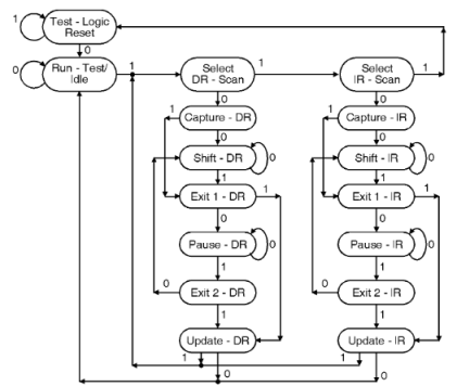
Test-Logic-Reset: This state is entered on power-up of the device. Run-Test-Idle: This state allows certain operations to occur depending on the current instruction. Select-DR-Scan: This state is entered prior to performing a scan operation on a data register. Select-IR-Scan: This state is entered prior to performing a scan operation on the instruction register. Capture-DR: This state allows data register selected by the current instruction on the rising edge of TCK. Shift-DR: This state shifts the data, in the currently selected register. Exit1-DR: This state allows the option of passing on to the Pause-DR state. Pause-DR: This wait state allows shifting of data to be temporarily halted. Exit2-DR: This state allows the option of passing on to the Update-DR state. Update-DR: This state causes data contained in the currently selected data register to be loaded into a latched parallel output. Capture-IR: This state allows data to be loaded from parallel inputs into the instruction register. Shift-IR: This shifts the values in the instruction register towards TDO. Exit1-IR: This state allows the option of passing on to the Pause-IR state. Pause-IR: This wait state that allows shifting of the instruction to be halted. Exit2-IR: This state allows the option of passing on to the Update-IR state. Update-IR: This state causes the values contained in the instruction register to be loaded into a latched parallel output on the falling edge of TCK after entering this state. Reference Books1. Allen Holberg, “Analog CMOS Design”, Oxford University Press.2. Neil H. E. Weste, David Money Harris, “CMOS VLSI Design: A Circuit & SystemPerspective”, Pearson Publication
- The stuck-at fault model.
- The transition delay fault (or transition fault) model, where the signal eventually assumes the correct value, but more slowly (or rarely, more quickly) than normal.
- Small-delay-defect mode.
From the above fig. Assume that the line α is s-a-1.Hence to test for α, both G3 = C = 1. Also D = G6 =1 so that G7 =1 if the fault is absent. To propagate the fault from G7 to output f via G8 requires G4 = 1.This is because if G4 = 0 then output f will be forced to be 1.The process of propagating the effect of the fault from its original location to the circuit output is known as forward trace.Similar is the process of backward trace. 6.6 Sequential Circuit TestATPG for sequential circuits. •variations required in fault model, algebra and ATPG procedure •compare the ATPG Complexity •A special scheme called “scan chain” which modifies a sequential circuit into a virtual combinational one”. When a circuit powers up, the flip-flops can have any value (0 or 1). •ATPG need to control (indirectly) the outputs of flip-flops and observe (indirectly) the inputs to the flip-flops. •Once achieved, ATPG for these combinational blocks can be done using D algorithm.•Single clock sequential circuits. •Each flip-flop is treated as 1-bit memory element with ONE common clock. •After a clock edge, the secondary output pattern (next state) is transferred to the output of the flip-flops (present state), which become new secondary inputs. Also, the primary outputs are updated. This activity occurs at each clock edge, and so it is called “synchronous” operation. •Single stuck at faults are assumed in NSF and OFB. •Internal faults of flip-flops are not modeled; their output and input faults are modeled as faults on input and output signals of the combinational blocks. •No faults are considered in the clock signal. •Most of the time, D-flip-flops are used in VLSI designs. So in this course whenever we refer to a flip-flop we essentially mean a D-flipflop. 6.7 BISTAs the complexity of VLSI circuits increases, test generation and application becomes an expensive and not always very effective means of testing. Built-in Self Test (BIST) is another solution. It is a mechanism that permits a machine to test itself. Engineers design BISTs to meet requirements such as: Advantages :Under normal operating conditions the cell is set so that it has no effect and it becomes invisible. However when the device is set to test mode, it permits a serial data stream (test vector) to be passed from one shift register latch cell to the next. Boundary-scan cells in a device can capture data from integrated circuit line, or force data onto them. In this way a test system that can input a data stream to the shift register chain can set up states on the board, and also monitor data. By setting up one serial data stream, latching this into place, and then monitor the returning data stream, it is possible to gain access to the circuits on the board and check that a returning data stream is what is expected. If it is, then the test can pass, but if not the boundary scan system has detected and problem that can be further investigated.JTAG InterfaceThere are a number of JTAG control and data lines that form the test access port, TAP. These lines known as TCK, TMS and the optional TRST line are connected in parallel to the chips in the boundary scan chain. Connections designated TDI (input) and TDO (output) are daisy chained together to provide a path around the boundary scan chips for the data. Data is sent into the TDI of the first chip, and then TDO from the first chip is connected to TDI of the next and so forth. Finally the data is taken from the TDO of the last IC in the daisy chain. 


0 matching results found
Browse by Topics