Unit - 5
Single Phase DC-AC converter
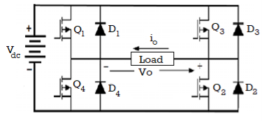
Full Bridge Voltage Source Inverter
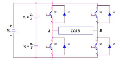
Fig:1 Circuit diagram of full bridge voltage source inverter
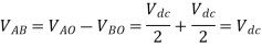
The above figure shows the power circuit of a full bridge VSI. This inverter is similar to the half bridge inverter, however a second leg provides the neutral point to the load. As in the half bridge inverter, both switches Q1 and Q2 or Q3 and Q4 in a single leg cannot be on simultaneously because a short circuit across the dc link voltage source Vdc would be occurred. In a full bridge inverter, there are four defined (states 1, 2, 3, and 4) switching states as shown in Table below. The undefined condition should be avoided so as to be always capable of defining the AC output voltage. It can be observed that the AC output voltage can acquire values up to the DC link value Vdc which is twice that obtained with half bridge voltage source inverter. Output voltage is denoted as VAB taken from the load.
The single-phase full bridge is similar to that of two half bridge circuits sharing the same DC bus. The full bridge circuit has two pole-voltages (VAO and VBO), which are similar to that of single phase inverter. Both voltages (VAO and VBO) of the full bridge circuit are square waves but they will have some phase difference.
State | Switching state | Output voltage | ||
 |  |  | ||
1 |  |  |  |  |
2 |  |  |  | 
|
3 |  |  |  | 0 |
4 |  |  |  | 0 |
State 1
In this state, the power switches Q1 and Q4 are in conduction mode and remaining switches are OFF condition. By using Thevenin’s analysis, pole voltages at ‘A’ and ‘B’ are (VAO and VBO) measured and the output voltage is VAB=VAO-VBO=VDC.
State 2
In this state, the power switches Q2 and Q3 are in conduction mode and remaining switches are in OFF condition. Pole voltages at ‘A’ and ‘B’ are measured from the load and the output voltage is determined by VAB=VAO-VBO= -VDC.
State 3
In this state, the power switches Q1 and Q3 are in conduction mode and remaining switches are in OFF condition. Voltages at nodes ‘A’ and ‘B’ are measured and the output voltage VAB=VAO-VBO= 0
State 4
In this state, the power switches Q2 and Q4 are in conduction mode and remaining switches are in OFF condition. Pole voltages at ‘A’ and ‘B’ are measured and a load voltage is calculated as VAB=VAO-VBO= 0
Key takeaway
State | Switching state | Output voltage | ||
 |  |  | ||
1 | 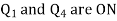 |  |  |  |
2 |  |  |  | 
|
3 |  |  |  | 0 |
4 | 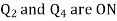 |  |  | 0 |
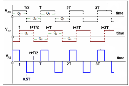
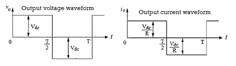
Fig:2 Output voltage waveform of full bridge inverter
The waveform indicates the representation of two pole voltages and load voltage wave forms of a full bridge single phase inverter. During the time period (0 to t), switches Q1 and Q4 are ON, and in which pole voltages are measured as
VAO=Vdc/2 and VBO=- Vdc/2.
Then output voltage (load voltage) is given by
Similarly, output voltage can be found for next three intervals.
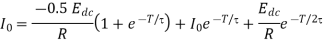
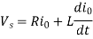
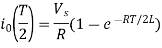
The time domain analysis of the steady state current waveform for a R-L load has been presented here. Under steady state the load current waveform in a particular output cycle will repeat in successive cycles and hence only one square wave period has been considered. Let t=0 be the instant when the positive half cycle of the square wave starts and let I0 be the load current at this instant. The negative half cycle of square wave starts at t=0.5T and extends up to T. The circuit equation valid during the positive half cycle of voltage can be written as below
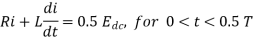
Similarly, the equation for the negative half cycle can be written as
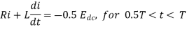
The instantaneous current ‘i’ during the first half of square wave may be obtained by solving above equation and putting the initial value of current as I0. Accordingly,  for
for  ….
….
Where =L/R is the time constant of the R-L load.
The current at the end of the positive half cycle becomes the starting current for the negative half cycle.
Thus, the next half cycle starts with an initial current =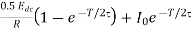
For 0.5T<t<T
Simplifying the above equation
 For 0.5T<t<T
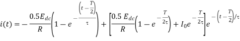
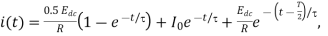
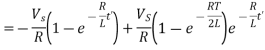
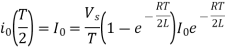
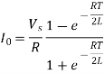
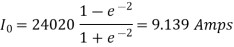
Under steady state, the instantaneous magnitude of inductive load current at the end of a periodic cycle must equal the current at the start of the cycle. Thus, putting t=T in above equation, one gets the expression for I0 as,

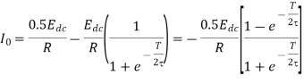
Substituting the above expression for I0
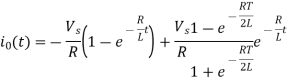
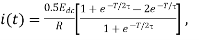 for 0<t<0.5 T
The load current at the end of the positive half cycle of square wave (at t=0.5T) simply turns out to be –I0. This is expected from the symmetry of the load voltage waveform. Load current expression for the negative half cycle of square wave can similarly be calculated by substituting for I0. Accordingly,
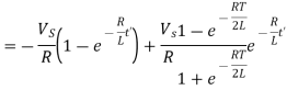
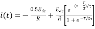 for 0.5 <t<T
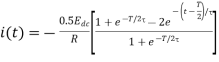 for 0.5 <t<T
Q1) (a) A single-phase full bridge inverter is connected to an RL load. For a dc source voltage of  and output frequency f=1/T, obtain expressions for load current as a function of time for the first two half cycles of the output voltage.
(b) Derive also the expressions for steady-state current for the first two half cycles.
(c) For R=20  and L=0.1H, obtain current expressions for parts (a) and (b) in case source voltage is 240 V dc and frequency of output voltage is 50 Hz.
A1)
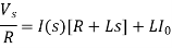
(a) For the first half cycle, for 0<t<T/2, the voltage equation for RL load is
Its Laplace transform, with zero initial conditions is
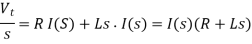
Its time solution is,
 0<t<T/2
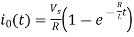
This is the expression of current as a function of time for the first half cycle from the instant of switching in with 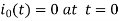
At  , current
  becomes the initial value of second half cycle.
For second half cycle, time limit is from T/2 to T or 0<t’ <T/2 where t’=t-T/2. The voltage equation for RL load during second half cycle is
It Laplace transform with initial current  given by
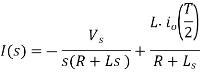
Its time solution is 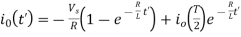
0 < t’ <T/2. The transient solution for load current for first and second half cycles respectively.
(b) Under steady-state conditions at t=0,  , under this condition Laplace transform
Its time solution is
At t=T/2 
Substituting this value of 
The steady-state solution during the first half cycle i.e., for 0<t<T/2
For second half cycle at t=T/2  , Under this initial condition,
Laplace transform0
The steady state solution during the second half cycle, i.e., for 0<t’<T/2 where t’=t-T/2
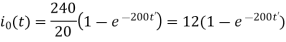
(c) Here 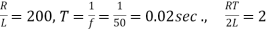
 during the first half cycle from
Expression for transient current for second half cycle,
Steady-state current for the first half cycle, i.e., for 0<t<T/2 is

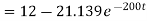
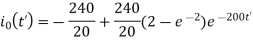
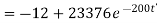
For the second half cycle, steady state current

 for 0<t’<T/2
Q2) A single phase bridge inverter delivers power to a series connected RLC load with R=2 and L=10
 The periodic time T=0.1 msec. What value of C should the load have in order to obtain load commutation for the SCRs. The thyristor turn-off time is 10sec. The circuit turn off time as 1.5
 assume that load current contains only fundamental component.
A2)
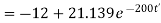
The value of C should be such that RLC load is underdamped. Moreover, when load voltage passes through zero, the load current must pass through zero, the load current must pass through zero before the voltage wae, i.e. The load current must lead the load voltage by an angle θ as shown if fig 8.6. Recall the phasor diagram for RLC series circuit. From this phasor diagram
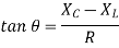
Here  as the current is leading the voltage. Now (θ/) must be at least equal to circuit turn-off time i.e., 1.5×10=15sec


The current source inverter (CSI) is a device that converts the input direct current into an alternating current. It is also called current fed inverter in which the output current is maintained constant irrespective of load on the inverter. This means that, the magnitude and nature of the load current depends on the nature of load impedance. The output voltage of the inverter is independent of the load. The major advantage of current source inverter is its reliability.
In the case of current source inverter, a commutation failure in the same leg does not occur due to the presence of a large inductance Ld connected in series with the voltage source.
Compared with a VSI system, the output current of a CSI system is not influenced by the supply voltage, so its output current has low THD and high PF.
Therefore, due to its advantages, the current source inverters are used in many industrial applications such as induction heating, static var compensators (SVC), variable speed a.c. motors etc.
The freewheeling diodes that are used for voltage source inverters become useless if an inverter is supplied from a d.c. Current source, this is because the current in any half-leg of the inverter cannot change its polarity, hence it can only flow through the power semiconductor switches. Therefore, absence of the freewheeling diodes reduces the size and weight of the inverter circuit.
Single-Phase Current Source Inverter
The following Fig(a) shows the circuit of a single-phase current source inverter. A constant current source is used here with a large value of inductance Ld in series with the current limited d.c. Voltage source Vdc.
The thyristors of the inverter circuits are, T1, T3, T2 and T4, are alternatively turned ON to obtain a nearly square wave current waveform. Two commutating capacitors – C1 in the upper half, and C2 in the lower half, are used.
Four diodes, D1, D2, D3 and D4 are connected in series with each thyristor to isolate the commutating capacitors from the load and prevent them from discharging through the load.
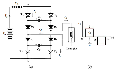
Fig 3(a) circuit of single phase CSI (b) output current waveform
Working
The output frequency of the inverter is controlled by varying the half time period, (T/2), at which the thyristors in pair are triggered by pulses being fed to the respective gates by the control circuit, to turn them ON. The operation of the circuit can be described as:
In the circuit of fig(a), two thyristors must trigger simultaneously to allow current to flow. For example, T1 and T3 must be triggered, while in reverse, T2 and T4 must trigger at the same time. The output current waveform is shown in fig(b) for the case of inductive load.
When T1 andT3 conduct, capacitors C1 and C2 would be charged with the polarity as shown. When T2 andT4 are turned on, thyristors T1 and T3 are reversed biased by the capacitors C1 and C2 respectively to commutate them. At this instant, the load current flows through T2 – C1 – D1 – load – D3 – C2 – T4 charging capacitors C1 and C2 with opposite polarity and are ready now to commutate T2 and T4, while the current in the load changes its direction and the cycle is repeated.
Three-Phase Current Source Inverter
The circuit of a three-phase current source inverter is shown in Fig. As in the circuit of a single-phase CSI, the input is also a constant current source. In this circuit, six thyristors, two in each of three arms, are used, as in a three-phase VSI. Also, six diodes D1, D2, D3, D4, D5 and D6, each one in series with the respective thyristor, are needed here, as used for single-phase CSI.
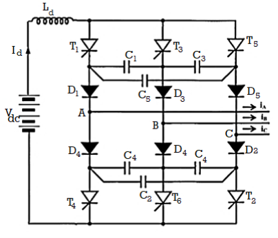
Fig:4 Circuit of three phase CSI
Six capacitors, three each in two (top and bottom) halves, are used for commutation. The six capacitors are equal, i.e., C1= C2 = C3.....= C6. The six diodes are needed in CSI, so as to prevent the capacitors from discharging through the load. Three Phase inverters are normally used for high power applications.
Modes of Operations
The three phase output can be obtained from a configuration of six switches and six diodes. Two types of control signals can be applied to the switches: 180°conduction or 1200 conduction.
1800 Conduction Mode
In these inverters each switch conducts for a duration of 1800. Three switches remain on, at any instant of time. When switch-1 is switched on, terminal 'a' is connected to the positive terminal of the DC input voltage.
When switch-4 is switched on, terminal 'b' is connected to the negative terminal of the DC source. There are six modes of operation in a cycle and the duration of each mode is 600. The switches are numbered in the sequence of gating the switches 1-2-3, 2-3-4, 3-4-5, 4-5-6, 5-6-1, 6-1 -2. The gating signals are shifted from each other by 600 to obtain three phase balanced voltages.
1200 Conduction Mode
In this conduction mode each switch conducts for 120". Only two switches remain on at any instant of time. The conduction sequence of switches is 6-1, 1-2, 2-3,3-4,4-5, 5-6, and 6-1. There are three modes of operation in a half cycle and the equivalent circuits.
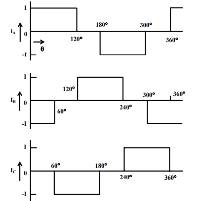
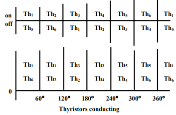
Fig:5 phase current waveform
Key takeaway
Comparison between VSI and CSI
Current Source Inverter | Voltage Source Inverter |
As inductor is used in the DC link, the source impedance is high. It acts as a constant current source. | As capacitor is used in the DC link. It acts as a low impedance voltage source. |
A CSI is capable of withstanding short circuit across any two of its output terminals. Hence complementary short circuit on load and misfiring of switches are acceptable. | A VSI cannot accept the misfiring of switches. |
CSI is used only buck or boost operation of inverter. VSI is used only buck or boost operation of inverter. |
|
The main circuit cannot be interchangeable. | The main circuit cannot be interchanged here also. |
It is affected by the EMI noise. | It is also affected by the EMI noise |
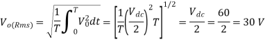
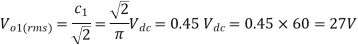
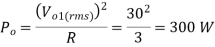
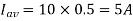
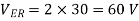
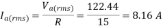
Ex.1 The single-phase half-bridge transistor inverter shown in Fig. Below has a resistive load of R = 3Ω and the d.c. Input voltage Vdc = 60 V. Determine:
(a) The rms value of the output voltage.
(b) The rms value of the load voltage at the fundamental frequency.
(c) The output power.
(d) The average and peak current of each transistor.
(e) The peak reverse blocking voltage VBR of each transistor.
(f) The total harmonic distortion factor.
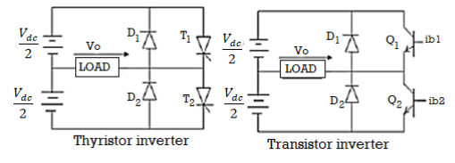
Ans:
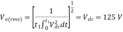
(a) The rms value of the output voltage is
(b) The rms value of the load voltage at the fundamental frequency is
(c) The output powr is
(d) The average and peak current of each transistor are
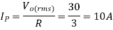
Because each transistor conducts for a 50% duty cycle, the average curret of each transistor is
(e) The peak reverse blocking voltage  of each transistor is
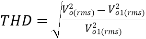
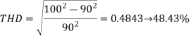
(f) The total harmonic distortion factor is
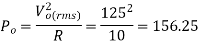
Ex.2 For the single-phase MOSFET bridge inverter circuit shown below, the source Vdc =125 V, load resistance R =10 Ω and output voltage frequency fo = 50 Hz.
a) Draw the output voltage and load current waveforms.
(b) Derive the rms value of the output voltage waveform and hence calculate the output power Po in terms of the output voltage.
(c) Analyse the amplitude of the Fourier series terms of the output voltage waveform by considering up to the 7th order harmonic. Determine the value of the rms output voltage in terms of harmonics rms values.
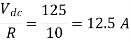
(d) Calculate the average and peak currents of each transistor.
(e) Estimate the total harmonic distortion factor THD of the circuit.
Ans:
(a)
(b) The rms value of the output voltage is
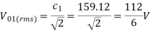
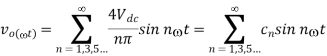
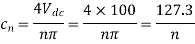
(c) The Fourier series of the output voltage is
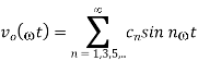
The amplitude  of the nth harmonic is:
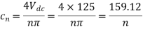


Hence the output voltage fourier representation is,

In terms of harmonics
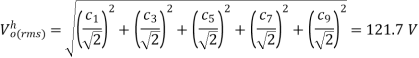
This value is less than  since we calculate up to 7th order harmonies only.
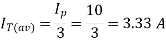
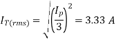
(d) Since the duty cycle of each transistor is 0.5, the current waveform is as shown below
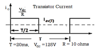
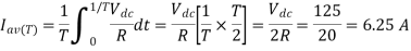
Peak current
(e)the total harmonic distortion factor.
 =
=
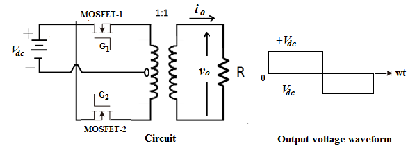
Ex.3 A single-phase MOSFET parallel inverter has a supply d.c. Voltage of 100V supplying a resistive load with R =10 Ω via a center-tap transformer with 1:1 ratio. The output frequency is 50 Hz.
(a) Draw the circuit diagram and the output voltage waveform of the inverter.
(b) Determine the rms value of the output voltage waveform.
(c) Determine the amplitude of the Fourier series terms for the square output voltage waveform up to 9th order harmonics.
(d) Calculate the rms value of the output voltage in terms of harmonic components that obtained in (b).
(e) Determine the power absorbed by the load consider up to 9th order harmonic.
(f) Draw the frequency spectra of the output voltage waveform.
(g) Calculate the total harmonic distortion factor THD.
Ans: (a) the circuit diagram and the output voltage waveform of the inverter
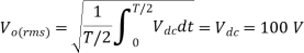
(b) The rms value of the output voltage is
(c) the Fourier series of the output voltage is
The amplitude cn of the n th order harmonic is:


Hence the output voltage Fourier representation is,

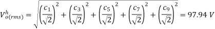
(d) In terms of the harmonics, the rms value of the output voltage is
(e) To calculate the power, we most calculate the rms value of the current for each harmonic the amplitude of the nth harmonic current

Where  =R
=R
 |  |  |  |  |  |
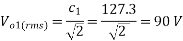
1 | 50 | 127.3 | 10 | 12.73 | 810 |
3 | 150 | 42.4 | 10 | 4.24 | 89.8 |
5 | 250 | 25.5 | 10 | 2.55 | 32.5 |
7 | 350 | 18.2 | 10 | 1.82 | 16.5 |
9 | 450 | 14.1 | 10 | 1.41 | 9.99 |
The total power is 
(f) The frequency spectrum is given in Fig.
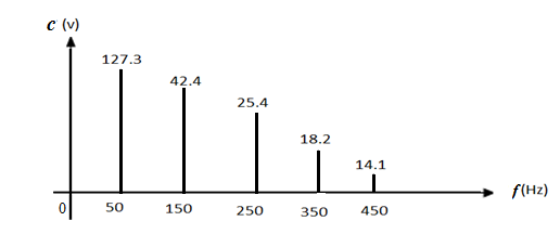
(g) The total harmonic distortion factor

This is very high THD, the practical value of THD is about (3-10) % hence we need to use low-pass filter at the output to filter out most of the undesirable harmonic component and to produce nearly sinusoidal output waveform.
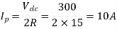
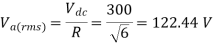
Ex.4 The three-phase inverter in Fig. Shown used to feed a Y-connected resistive load with R =15 Ω per-phase. The d.c. Input to the inverter Vdc = 300 V and the output frequency is 50 Hz. If the inverter is operating with 120˚ conduction mode, calculate: (a) The peak and rms value of the load current IL, (b) The output power, and the average and rms values of the current of each transistor.
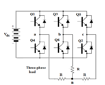
Ans:
(a) For 120ᵒ conduction mode, at any time the load resistances of two phases are connected in series, hence, peak value of load current is
The rms value of the phase voltage is
Hence the rms value of the load current is
(b) The load power is

(c) For 120ᵒ conduction mode, each transistor carries current for (1/3) rd of a cycle, hence the average transistor current is
The rms value of the thyristor current is
When there are AC loads it requires the voltage to be maintained or controlled at the input terminals. When inverters are used for such loads, we ned the output voltage to be in control. Because the requirements of AC loads can be fulfilled.
(a) External control of AC output voltage:
This can be done by AC voltage control in which an ac voltage controller is connected in between the output terminals of inverter and the load. The below figure shows the connections. The voltage input to the ac load is regulated through the firing angle control of ac voltage controller. But there are harmonics in the output when the output voltage from the ac voltage controller is at low level.
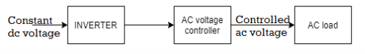
Fig 6
The other method is series inverter method which consists of two or more inverters which are connected in series. Figure below shows that the output voltage of two inverters is summed with the help of transformer. The secondaries of the transformer are connected in series having input as the inverters output. The resultant voltage from the phasor is then
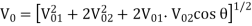
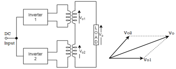
Fig 7 Series Inverter Control of two inverters
The essential condition for this is V01, V02 should be equal.
When  =0
=0
V0= V01+ V02
When  =π
=π
V0 = 0 only when V01= V02
As inverters are connected in series this method is also called as multiple converter control.
(b) External control of dc Input Voltage
AC voltage source is present here. The input to the converter which is dc voltage is controlled through the fully controlled rectifier (a). Alternate method is to use an uncontrolled rectifier and a chopper (b). The other way is to use an ac voltage controller and an uncontrolled rectifier (c). If the available volage is dc then dc voltage input to the inverter is controlled by means of a chopper as shown in figure below.
Fig 8 External control of dc input voltage to inverter
The output voltage waveform and its harmonics are not affected as the output voltage of inverter is controlled through the adjustment of dc input to the inverter.
(c) Internal control of Inverter
By adjusting the voltage within the inverter, the output voltage can be adjusted. The is can be achieved by pulse width modulation control (PWM). In PWM method the inverter is fed with fixed dc input voltage and a controlled ac output voltage is obtained by adjusting the ON and OFF periods of the inverter.
No additional components are required to adjust the voltage. The lower harmonic orders are also eliminated. The higher order harmonics can be filtered easily. The main disadvantage of this method is that the SCR are expensive as they must possess low turn on and turn off times.
Key takeaway
When there are AC loads it requires the voltage to be maintained or controlled at the input terminals. When inverters are used for such loads, we ned the output voltage to be in control. Because the requirements of AC loads can be fulfilled.
The output voltage quality is the basic advantage of voltage source inverters (VSI) for UPS systems. The sinusoidal PWM is typical for single- or three-phase UPS systems while space vector modulation is the standard in three-phase induction motor control systems. Single-phase inverters with output power up to 3 ÷ 4 kVA are typical for a UPS for computer systems. So, the demands on them should be precisely established. The EN 62040-3 standard limits the Total Harmonic Distortion (THD) of the output voltage for the defined nonlinear load and presents the requirements for the transient response depending on the class of the system.
The IEEE 519 standard specifies the demands concerning the maximum THD and the highest harmonic amplitude of the supplied voltage in the steady state. Considering the output voltage harmonics of the PWM inverter it can be easily proved that the harmonic with the highest amplitude before filtering has the frequency fc (fc - frequency of the modulated waveform) or fc±fm (fm - fundamental frequency of the modulating sinusoidal signal) where fc>50fm is usual in UPS systems. The design of the output filter is based on the requirement to sufficiently suppress them and to minimize the reactive power in the output filter components. The IEEE-519 standard does not specify the limit of the highest order of the harmonic spectrum considered. So, it can be used for the design of the output filter.
The EN 62040-3 standard presents demands for the low frequency harmonics (<40) at the supplied voltage. The low-order harmonics can be reduced practically only by means of the feedback loop. That is why the EN 62040-3 standard is useful for the assignment of control loop requirements. The 3-phase inverters control for a balanced load can be easily designed using the Clarke transform where a 3-phase control system is changed into two orthogonal single-phase systems. An interesting approach is presented in where the three-phase three-legged VSI is decoupled into two buck converters in every 60° region.
Two types of inverter control systems can be considered. The traditional control systems based on the discrete model of the inverter and the fuzzy control system based on "control rules". The presented discrete PID controller has its origin in a continuous controller; deadbeat controller is unique for discrete systems and has some parameters (the control speed) that are unreachable in continuous systems but it is more sensitive to load changes. The aim of this paper is to show how the different types of the control systems influence on the output voltage quality of single-phase, 3-level voltage source inverter for a standard nonlinear load.
Fig 9 A single phase inverter with non linear load
The distortions of the output voltage depend on the design of the output filter. The output filter design was presented in and was based on the approach. The reduction of the highest amplitude of harmonics (close to fc frequency) below 3%, and THD below 5% (IEEE-519) was the assumption of the output filter LFCF product value calculation. The particular LF and CF values (for the known LFCF product value) were calculated to minimize the reactive power in the output filter components The considerations in this paper are limited only to single-phase 3-level VSI with a double edge PWM. The simplified calculation of the LF and CF output filter parameters is
Where VOUTRMS and IORMS are the rms values of the inverter output voltage and current. The calculated values in the presented example are LF=1.8 mH (RLF=0.5 Ω), CF=0.85 µF, RCF=0. The design of the output filter has a strong influence on the discrete model of the inverter and as a result on the design of the controller. Most authors that present control techniques in inverters significantly lower the value of the filter inductance and increase the value of the filter capacitance because the value of the output inverter impedance is proportional to LF/CF ratio. The LF value determines how fast the output capacitor CO can be charged when the rectifier forward bias begins. Figure below shows the output voltage waveform of the inverter without the feedback loop for a nonlinear load.
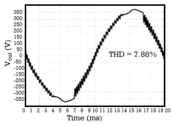
Fig 10 Output voltage distortion for standard non-linear load.
When the reverse bias of the rectifier begins, the oscillating waveform that has the angular frequency ωRB=1/√(LFCF) and the dumping factor ξRB=0.5ωRBRLFCF is subtracted from the output sinusoidal voltage. When the forward bias of the rectifier begins, the oscillating waveform that has the angular frequency ωFB=1/√(LFCO) and
The dumping factor
ξFB=0.5[ωFBLF/RO+ωFB(RLF+RS) CO] is subtracted from the output sinusoidal voltage. The simplified analysis of the possibility of output voltage distortion lowering is based on the calculation of the desired voltage waveform on the input of the filter to get the sinusoidal waveform on the output of the inverter with a nonlinear load. It is not possible to force a sufficiently high step increase of the input voltage of the output filter when the forward bias of the rectifier begins in any control system for the output filter inductance LF>LFmax,
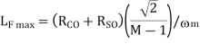
Where ωm=2πfm, M is the modulation ratio in the operating point of the inverter, RCO is an ESR of the load capacitor and RSL is a sum of all the serial resistances of the nonlinear load. In a case where RCO+RSO≈RS=2 Ω, M=0.8, fm=50 Hz the inductance is LFmax≈5 mH. When the rectifier is forward biased the current charging the load capacitor CO should be forced and further this current should be reduced, or for a high value of CO this current should change its sign. Owing to the rectifier, the capacitor CO can be discharged only through the load resistance RO and for a high value of CORO no control system can discharge the load capacitor faster. Only systems that remember the previous fundamental cycle (e.g. the repetitive controller) or that additionally control the inductor and output currents (the multi-input deadbeat controller) can effectively reduce this type of the output voltage error. Fig. Above presents the output voltage of the VSI with an open feedback loop and a nonlinear rectifier RC load.
References:
- Vedam Subramanyam - Power Electronics, New Age International, New Delhi.
- Dubey, Donalda, Joshi, Sinha, Thyristors Power controllers, Wiley Eastern New Delhi.
- M. D. Singh and K. B. Khandchandani, Power Electronics, Tata McGraw Hill.
- Jai P. Agrawal, Power Electronics systems theory and design LPE, Pearson Education, Asia.
- L. Umanand, Power Electronics – Essentials and Applications Wiley Publication.
- J. Michael Jacob – Power Electronics Principal and Applications.
- M. H. Rashid - Power Electronics Handbook, Butterworth-Heinemann publication, 3rd edition


