Unit - 4
Three Phase Converter and AC Voltage Regulator
A three phase fully controlled converter is obtained by replacing all the six diodes of an uncontrolled converter by six thyristors as shown in Figure 1.
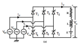
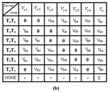
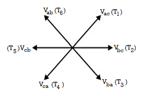
Figure 1. Operation of Fully controlled three phase converter.
(a) Circuit diagram
(b) Conduction table
(c) Phaser diagram of line voltages
- For any current to flow in the load at least one device from the top group (T1, T3, T5) and one from the bottom group (T2, T4, T6) must conduct
- Now the thyristors are fired in the sequence T1 → T2 → T3 → T4 → T5 → T6 → T1 with 60° interval between each firing. Therefore, thyristors on the same phase leg are fired at an interval of 180° and hence cannot conduct simultaneously.
- This leaves only six possible conduction mode for the converter in the continuous conduction mode of operation. These are T1T2, T2T3, T3T4, T4T5, T5T6, T6T1. Each conduction mode is of 60° duration and appears in the sequence mentioned.
- The conduction table of Fig. (b) shows voltage across different devices and the dc output voltage for each conduction interval.
- The phasor diagram of the line voltages appears in Fig. (c). Each of these line voltages can be associated with the firing of a thyristor with the help of the conduction table 1.
- For example, the thyristor T1 is fired at the end of T5T6 conduction interval. During this period, the voltage across T1 was Vac. Therefore, T1 is fired α angle after the positive going zero crossing of Vac.
- The phasor diagram of Fig. (c) also confirms that all the thyristors are fired in the correct sequence with 60° interval between each firing.
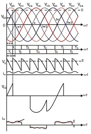
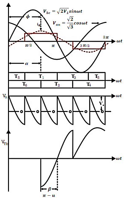
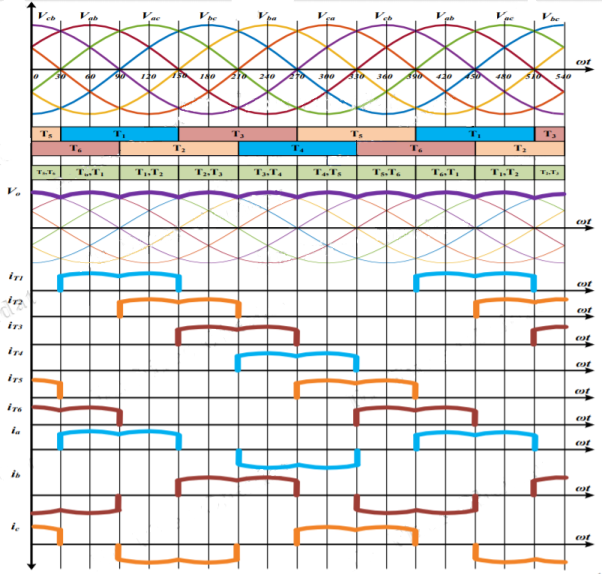
Figure 2. Wave forms of three phase fully controlled converter
- Fig. 2 shows the waveforms of different variables. To arrive at the waveforms, it is necessary to draw the conduction diagram which shows the interval of conduction for each thyristor and can be drawn with the help of the phasor diagram of fig1 (c).
- If the converter firing angle is α each thyristor is fired “α” angle after the positive going zero crossing of the line voltage with which it’s firing is associated.
- Once the conduction diagram is drawn all other voltage waveforms can be drawn from the line voltage waveforms and from the conduction table of fig. 1 (b).
- Similarly, line currents can be drawn from the output current and the conduction diagram.
- It is clear from the waveforms that output voltage and current waveforms are periodic over one sixth of the input cycle. Therefore, this converter is also called the “six pulse” converter.
- The input current on the other hand contains only odds harmonics of the input frequency other than the triplex (3rd, 9th etc.) harmonics.
Analysis of the converter in the rectifier mode
The output voltage waveform can be written as
Vo = Vo +  AK cos 6K wt +
  BK sin 6K wt
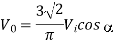
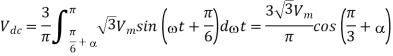
Vo = 3/π  dwt = 3 √2 / π VL
 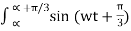 dwt
dwt
= 3 √ 2 / π V L cos α
VAK = 6/ π  cos 6K wt dwt
= 6/ π  VL sin (wt + π /3) cos 6 wt d wt
= 3 √ 2 / π VL [ cos (6K +1) α/ 6K + 1 – cos (6K -1) α / 6K -1]
VBK = 6/
 sin 6 Kwt dwt
= 6/ 
 VL sin (wt + π/3) sin 6 wt dwt
= 3√2/π VL [sin(6K +1) α / 6K + 1 – sin(6K-1) α/ 6K-1]
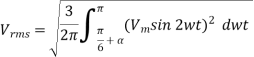
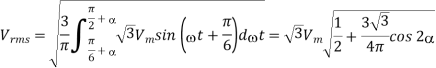
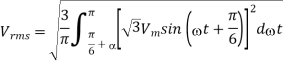
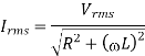
V(RMS) = √ 3/π  2 d wt
= VL [ 1 + 3√3 / 4π cos 2α] ½
The input phase current is expressed as
Ia= io α ≤ wt ≤ α + π/3
Ia = -io α + 2π/3 ≤ wt ≤ α + 4π/3
Ia= io α + 5π/3 ≤ wt ≤ α + 2π
Ia=0 otherwise
From Fig. 2 it can be observed that io itself has a ripple at a frequency six times the input frequency. However, if io is replaced by its average value Io. This approximation will be valid provided the ripple on i0 is small, that is the load is highly inductive. The modified input current waveform will be ia which can be expressed in terms of a Fourier series as
Ia ≈  = IA0/2
  cos n wt +
  sin n wt
Where
IA0 = 1/2π  dwt = 0
I AB = 1/ π  cos n wt n ≠ 0
= 4I0/ n π cos nπ/6 sin nπ/2 cos nα
I AB = (-1) K 2√3 Io/ (6K± 1) α
For n=6K± 1, K = 0,1,2,3 ………..
I AB = 0 otherwise.
I Bn = 1/ π  sin nwt dwt
= 4I0 / n π cos nπ/6 sin nα sin n π/2
Ibn = (-1) k 2√3/I0 /(6K ± 1)π sin(Kπ ± π/2) sin(6K± 1)α
For n = 6K ± 1, K=0, 1, 2……..
Ibn = 0 otherwise
Therefore,
Ia =  Io (-1) k / (6K ± 1) π sin(Kπ ± π/2) cos[ (6K ± 1) (wt – α)]
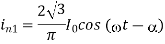
In particular ia1 = fundamental component of ia = 2√3 / π Io cos(wt-α)
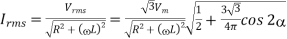
Van = √ 2 VL / √ 3 cos wt
Displacement angle Ø = α
Displacement factor = cos α
Distortion factor = Ia1/Ia = (√6/π) Io / √2/3 Io = 3/π
Power factor = Displacement factor x Distortion factor = 3/ π cos α
The closed form expression for io in the interval α ≤ wt ≤ α + π/3 can be found as follows in the interval,
R io + L dio/dt + E = vo = √ 2 VL sin(wt + π/3)
Io= I1 e –(wt – α) / tan Ø + √ 2 VL/ Z sin(wt + π/3 -Ø) – E/R
Where Z = √ R2 + w 2 L 2, tan Ø = wL/R
R = Z cos Ø, E = √ 2 VL sin(wt + π/3) from figure 2.
Io = I1 e –(wt - α) / tan Ø + √2 VL/Z [ sin wt + π/3 – Ø] – sin Ѳ/ cos Ø
Since io is periodic over π/3
Therefore, I1 + √ 2 VL / Z [sin (α + π/3 –  ) – sin Ѳ / cos
  ]
]
= I1 e π/ tan  + √ 2 VL / Z [sin(α + π/3 – Ø) – sin Ѳ/ cos
  ]
]
Or
I 1 =√ 2 VL / Z sin ( / 1 – e π/3 tan
Io = √ 2 VL / Z [ sin ( / 1 – e π/ 3tan
  + sin(wt + π/3 -Ø) – sin Ѳ/ cos Ø]
Analysis of the converter in the inverting mode
In all the analysis it has been assumed that α < 90°. It is seen that the output dc voltage will be positive in this case and power will be flowing from the three- phase ac side to the dc side. This is the rectifier mode of operation of the converter.
However, if α is made larger than 90° the direction of power flow through the converter will reverse provided there exists a power source in the dc side of suitable polarity. The converter in that case is said to be operating in the inverter mode.
It has been explained in connection with single phase converters that the polarity of EMF source on the dc side would have to be reversed for inverter mode of operator.
Fig. 3 shows the circuit connection and wave forms in the inverting mode of operation where the load current has been assumed to be continuous and ripple free.
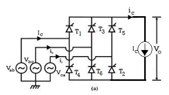
Figure 3. Inverting mode
(b) Wave forms in inverter mode of operation
Analysis of the converter in the inverting mode is similar to its rectifier mode of operation. The same expressions hold for the dc and harmonic compounds in the output voltage and current.
The input supply current Fourier series is
For values of α in the range 90° < α < 180° it is observed from Fig. 3(b) that the average dc voltage is negative and the displacement angle φ of the fundamental component of the input ac line current is equal to α > 90°.
Therefore, power in the ac side flows from the converter to the source. It is observed from Fig. 3(b) that an outgoing thyristor (thyristor T6 in Fig. 3(b)) after commutation is impressed with a negative voltage of duration β = π – α.
For successful commutation of the outgoing thyristor it is essential that this interval is larger than the turn off time of the thyristor i.e, β ω≥ tq , tq is the thyristor turn off time Therefore π - α ω≥ ≤ tq or α π -ωtq which imposes an upper limit on the value of α. In practice this upper value of α is further reduced due to commutation overlap.
Problems:
A three phase fully controlled bridge converter operating from a 3-phase 220V , 50Hz supply is used to charge a battery bank with nominal voltage of 240V. The battery bank has internal resistance of 0.01Ω and the battery bank voltage varies by ± 10% around its nominal value between fully charges and uncharged condition. Assuming continuous conduction find out:
- The range of firing angle of the converter
- The range of ac input power
- The range of charging efficiency.
When the battery bank is charged with constant average charging current of 100Amps through a 250mH lossless inductor.
The maximum and miminum battery voltages are VB(min) = 0.9 x VB Nom = 216 volts
And VB (max) = 1.1 x VB Nom = 264 volts.
Since the average charging current is constant 100A.
Vo (max) = V B max + 100 x RB = 264 + 100 x 0.01 = 265 volts
Vo (min) = VB (min) + 100 x RB = 216 + 100 x 0.01 = 217 volts.
But Vo max = 3√ 2/ π VL cos α min ; α min = 26.88
Vo min = 3√ 2/ π VL cos α max α max = 43.08
Therefore pf max = Distortion factor x displacement factor | max = 3/ π x cos α min = 0.85
p.f Min = 3/π x cos α max = 0.697
(iii) Power loss during charging = Io 2 RMS RB
But Io RMS 2 = Io 2 + I1 2 + I2 2 +………. And Ik ≈ VK / 6K wL = √ V 2 AK + V 2 BK / 6√2 K wL
For α = α min
VA1 = 0.439V VB1 = 48.8 V I1 = 0.073 Amps
VA2 = 10.76 VB2 = 20.15 I2 = 0.017 Amps
Jo 2 rms ≈ 100 2 +(0.073) 2 + (0.017) 2 = 10000.00562
Ploss = 100 watts.
At α min Po = Io x Vb max 26400 watts
Charging effeiency = 26400/26400 + 100 = 99.6%
For αmax Io 2 rms = Io 2
Ploss = 100 watts
Po = Vo x Vb min = 21600 watts
Charging effeciency = 21600/ 21600 + 100 = 99.54 %
A three phase fully controlled converter operates from a 3 phase 230 V, 50 Hz supply through a Y/Δ transformer to supply a 220 V, 600 rpm, 500 A separately excited dc motor. The motor has an armature resistance of 0.02 Ω. What should be the transformer turns ratio such that the converter produces rated motor terminal voltage at 0º firing angle. Assume continuous conduction. The same converter is now used to brake the motor regeneratively in the reverse direction. If the thyristors are to be provided with a minimum turn off time of 100 μs, what is the maximum reverse speed at which rated braking torque can be produced.
Form the above 3√2 / π VL = 220 V ; VL = 162.9V
Where VL is the secondary side line and also phase voltage since the secondary side is ∆ connected.
Primary side phase voltage = 230/√3 = 132.79V
Turns ratio = 132.79/162.9 = 1:1.2267
During regenrative braking in reverse direction the converter operates in the mode.
Tq| min = 100 µ sec
Β min = wtq| min = 1.8 0
Α max = 180 – β min = 178.2 0
The maximum negative voltage that can be generated by the converter is 3√2/π V L cos 178.2 = -219.89V
For rated braking torque Ia = 500 A
Eb = Va – Ia r = -229.89 V
At 600 RPM Eb= 220 – 500 x 0.02 = 210V
Maximum reverse speed is 229/210 x 600 = 656.83 RPM.
Key takeaway
A three phase fully controlled converter is obtained by replacing all the six diodes of an uncontrolled converter by six thyristors.
The input phase current is expressed as
Ia= io α ≤ wt ≤ α + π/3
Ia = -io α + 2π/3 ≤ wt ≤ α + 4π/3
Ia= io α + 5π/3 ≤ wt ≤ α + 2π
Ia=0 otherwise
Fig. 4(a) shows the circuit diagram of three phase half- controlled converter supplying an R-LE load. In the continuous conduction mode only one thyristor from top group and only one diode from the bottom group conduct at a time. However, unlike fully controlled converter here both devices from the same phase leg can conduct at the same time. Hence, there are nine conducting modes as shown in Fig. 4(b).
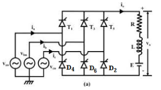
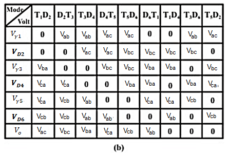
Figure 4 . Half fully controlled three phase circuit and condution diagram
- Consider the conducting and blocking state of D2. In the blocking state the voltage across D2 is either Vac or Vbc. Hence, D2 can block only when these voltages are negative.
- Taking Vbc as the reference phasor (i.e., Vbc = 2V sinωt ) D2 will block during 2π/3 ≤ ωt ≤2π and will conduct in the interval 0 ≤ ωt ≤2π/3 .
- Similarly, it can be shown that D4 and D6 will conduct during 2π/
- 3 ≤ ωt ≤ 4π/3 and 4π/3 ≤ ωt≤ 2π respectively. Next consider conduction of T1. The firing sequence of the thyristor is T1 → T3 → T5. Therefore, before T1 comes into conduction T5 conducts and voltage across T1 is Vac= 2V sin (ωt + π/3).
- If the firing angle of T1 is α then T1 starts conduction at ωt = α - π/3 and conducts up to α + π/3. Similarly T3 and T5 conducts during α + π/3 ≤ ≤ ωt α + π and α + π ω≤ ≤t 2π + α - π/3.
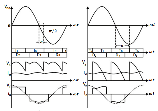
Figure 5. Waveforms of three half phase controller with α =  α =
α = 
Key takeaway
In the continuous conduction mode only one thyristor from top group and only one diode from the bottom group conducts at a time. However, unlike fully controlled converter here both devices from the same phase leg can conduct at the same time. Hence, there are nine conducting modes
The Three- phase half – wave controlled rectifier is shown in Fig. 6 .As for the half – wave 3-phase uncontrolled diode rectifier, the load is connected between the converter positive terminal (cathodes of all thyristors) and the supply neutral. The diode with the highest voltage w.r.t. The neutral conducts. As the voltage of another diode becomes the highest, the load current is transferred to that device, and the previously conducting device is reverse biased and naturally commutated. The waveforms for the supply voltage, output voltage, and load current are shown in Fig.7.
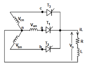
Figure 6. Three phase half wave controlled with R-L load.
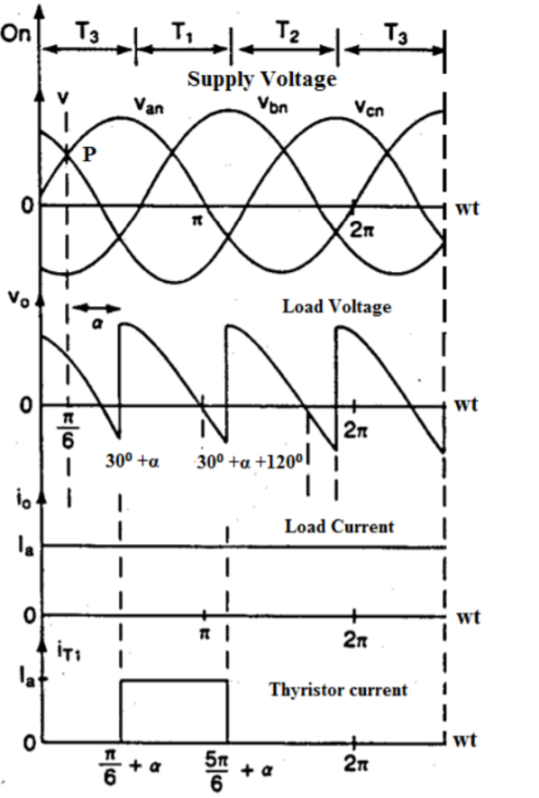
Figure 7. Waveforms
The average value of the output voltage Vdc can be found as:
Let van= Vm sin ωt
Vbn = Vm sin( ωt - 2 π / 3)
Vcn = Vm sin( ωt - 4 π / 3)
The average value of the load voltage wave is
𝑉𝑑𝑐 = 1 / 2𝜋/ 3 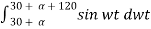 = 3Vm/2π [-cos(150 + α] – cos( 30 + α)]
= 3Vm/2π [ - (- √3/2 - √3/2) cos α] = 3 √3 Vm 2π cos α.
The load current  is
is
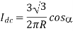
The operation of the 3 – phase half – wave rectifier with different values of α is illustrated in Fig.8. It can be seen that this converter can operate either as a rectifier or as an inverter as For 0⁰ < α < 90⁰ Rectifier 90⁰ < α < 180⁰ Inversion
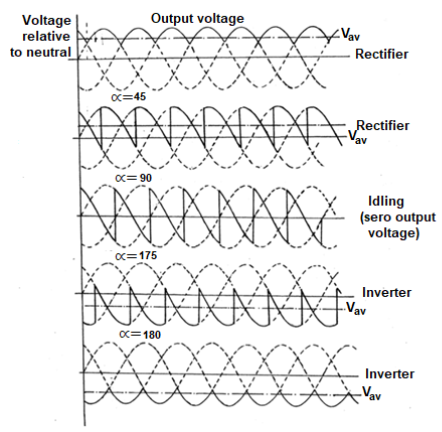
Figure 8. Output for different firing angles
R load
When the load is resistive, current id has the same waveform of the load voltage. As the load becomes more and more inductive, the current flattens and finally becomes constant. The thyristor goes to the non-conducting condition (OFF state) when the following thyristor is switched ON, or the current, tries to reach a negative value.
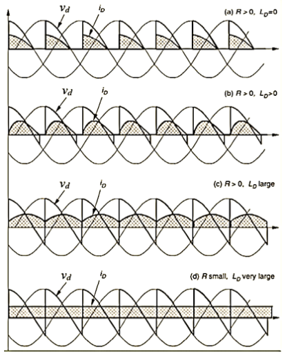
Figure 9. Resistive load
Firing angle:
Figure 10. Resistive load
- 0°<=α<=30º, output voltage is continuous.
- 30°<=α<=120º, output voltage is discontinuous and has some intervals in which output voltage is zero.
- α >150°, output voltage is zero.
In the case of a three-phase half wave controlled rectifier with resistive load, the thyristor T1 is triggered at ωt=(30°+α) and T1 conducts up to ωt=180°. When the phase supply voltage decreases to zero, the load current falls to zero and the thyristor T1 turns off. Thus T1 conducts from ωt=(30° + α) to (180°).
When α ≤ 30
Vdc = 3/2π  m sinwt dwt = 3√3 Vm/ 2π cos α.
Idc = Vdc / R = = 3√3 Vm/ 2π R cos α.
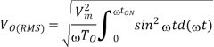
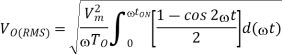
Vrms = 3/ 2π  m sinwt) 2 dwt = √3 Vm √ 1/6 + √3/8π cos 2α
Irms = Vrms/R = √3 Vm/R √ 1/6 + √3/8π cos 2α
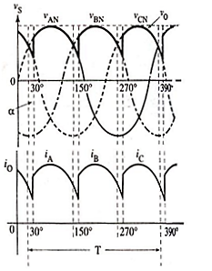
Figure 11. Waveform
when α≥30 o
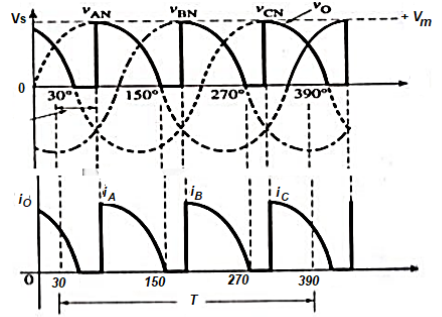
Figure 12. Waveform
Vdc = 3/2π  m sin wt dwt = 3 Vm/2π (1+ cos(
Idc = Vdc /R = 3Vm/ 2π R (1+ cos(π/6 + α))
= √ 3 Vm2 / 4 π 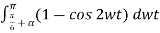
= Vm √ 3/4
I rms = Vrms / R = = Vm/ R √ 3/4
Operation of full converter with R -L load
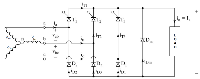
Figure 13. R-L load full converter
Three phase full converter is a fully controlled bridge- controlled rectifier using six thyristors connected in the form of a full wave bridge configuration. All the six thyristors are controlled switches which are turned on at a appropriate times by applying suitable gate trigger signals.
If T1 is triggered at (30 + ), T3 will be triggered at (30 + +120) and T5 will be triggered at (30 + +240). T4 will be triggered at (30 + +180), T6 will be triggered at (30 + +120+180) and T2 will be triggered at (30 + +240+180).
Firing angle |  |  |  |  |  |  |
 | 30  | 90  | 150  | 210  | 270  | 330  |
30  | 60  | 120  | 180  | 240  | 300  | 360  |
60  | 90  | 150  | 210  | 270  | 330  | 390  |
90  | 120  | 180  | 240  | 300  | 360  | 420  |
When α = 0
When α = 30
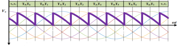
Figure 14. Output waveforms
When α = 60
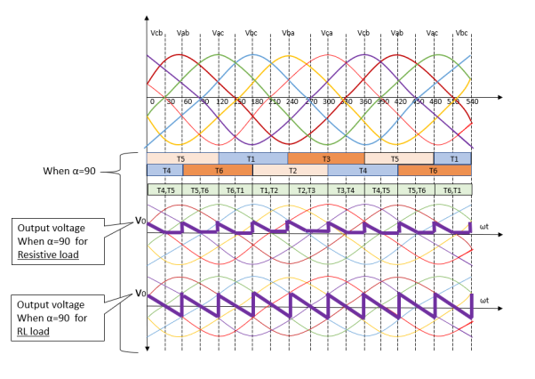
Figure 15. Output wave forms
Let V𝑎𝑛 = 𝑉𝑚sin𝜔t
𝑉𝑏𝑛 = 𝑉𝑚sin(𝜔t-2π/3)
𝑉𝑏𝑛 = 𝑉𝑚sin(𝜔t-4π/3)
The dc component of the output voltage and current can be found asp
The rms component of the output voltage and current waveforms are determined from
Special case: resistive load α˃60 o
The dc component of the output voltage and current can be found as
The rms component of the output voltage and current waveforms are determined from
Key takeaways
The Three- phase half – wave controlled rectifiers for the half – wave 3-phase uncontrolled diode rectifier, the load is connected between the converter positive terminal (cathodes of all thyristors) and the supply neutral. The diode with the highest voltage w.r.t. the neutral conducts. As the voltage of another diode becomes the highest, the load current is transferred to that device, and the previously conducting device is reverse biased and naturally commutated.
Problems:
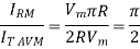
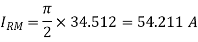
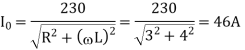
A three phase controlled rectifier has input voltage which is 480Vrms at 60Hz . The load is modelled as a series resistance and inductance with R = 10 Ω and L = 50mH. Determine the delay angle required to produce an average current of 50A in the load.
Vdc = Idc . R = 50 x 10 = 500V
√ 3 Vrms = 480V
α= cos -1 Vdc π / 3 √3 Vm = cos -1 ( 500 π/ 3 √24 80) = 39.5 0
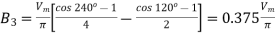
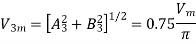
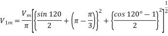
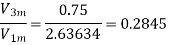
Power factor=Displacement factor×Distortion factor=THD=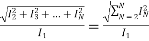
TUF

Where  RMS supply (secondary voltage
 RMS supply (secondary ) current
Average output voltage
RMS Load Voltage Vo=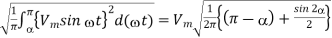
RMS Load Current =Vo/R
Average Load Voltage=0
 +cos 0]
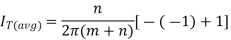
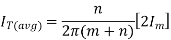

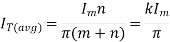
Where  maximum or peak thyristor current.
RMS current of thyristor 
RMS output voltage
Output RMS Voltage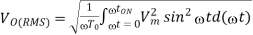
Substituting for 
Now  An integral number of input cycles; hence

Where T is the input supply time period (T=input cycle time period). Thus we note that 
Where 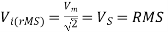 value of input supply voltage;
Problem:
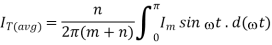
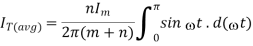
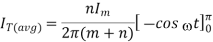
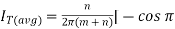
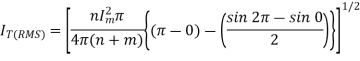
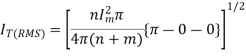
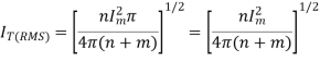
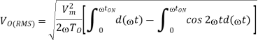
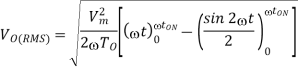
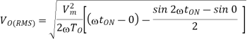
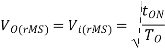
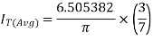
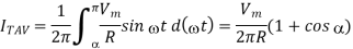
A single- phase full wave ac voltage controller working on ON-OFF control technique has supply voltage of 230V, RMS 50Hz, load = 50Ω. The controller is ON for 30 cycles and off for 40 cycles. Calculate
• ON & OFF time intervals.
• RMS output voltage.
• Input P.F.
• Average and RMS thyristor currents.
Solution:
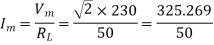
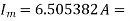
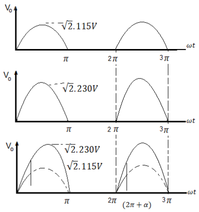
Vin(rms) = 230V; Vm = √ 2 x 230 = 325.269 V, Vm = 325.269 V
T = 1/f = 1/50 = 0.02 sec; T = 20 ms
n = number of input cycles during which controller is ON; n = 30
m = number of input cycles during which controller is OFF; m=40
TOn = n x T = 30 x 20 ms = 0.6 se
Controller ON time
TOFF = m x t = 40 x 20 ms = 800 msec = 0.8 sec
TOFF = controller OFF time.
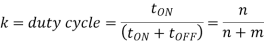
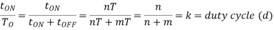
Duty cycle k = n/ (m+n) = 30/40 + 30 = 0.4285
RMS output voltage:
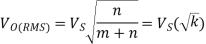
Vo(rms) = Vi(rms) x √ n/(m+n)
= 230 x √ 30 / 30 + 40 = 230 √ 3/7 = 150.570V
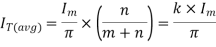
Io(rms) = Vo(rms) / Z = Vo(rms) / RL = 150.570/50 = 3.0114A
Po = Io 2 (rms) x RL = 3.0114 2 x 50 = 453.426498W
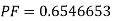
Input power Factor 
 =
=
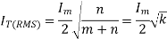
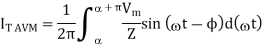
Average Thyristor current Rating
 Peak (maximum) thyristor current
RMS Current Rating of Thyristor
Q1) A single phase voltage controller has input voltage of 230V, 50Hz and a load R=15 . For 6 cycles on and 4 cycles off determine (i) rms output voltage (ii) input pf (iii) Average and rms thyristor currents?
A1)
(a) rms value of output voltage is
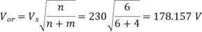
(b) input pf=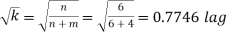
Also power delivered to load 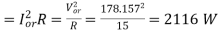
Input VA 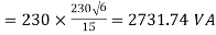
 Input pf=
(c) peak thyristor current, 
Average value of thyristor current
Rms value of thyristor current
Q2) A single-phase voltage controller feeds power to a resistive load of 3 from 230V, 50Hz source. Calculate:
(a) the maximum values of average and rms thyristor currents for any firing angle ,
(b) the minimum circuit turn-off time for any firing angle ,
(c) the ratio of third-harmonic voltage to fundamental voltage for  ,
,
(d) the maximum value of di/dt occurring in the thyristors,
A2)
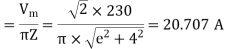
a) It is seen current through thyristor flows from to π for the first cycle of 2π radians. Therefore, average thyristor current is given by
Its maximum value occurs at =0. Therefore maximum value of average thyristor current is
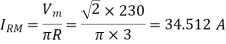
Rms thyristor current is
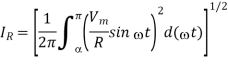
Its maximum value occurs at =0

(b) Waveforms for  show that for any value of firing angle the circuit turn-off time is always π radians.
Circuit turn-off time=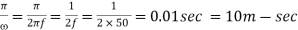
(c) for third harmonic
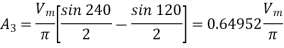
The amplitude of third harmonic voltage from eq 9.12 is
The amplitude of fundamental frequency voltage from eq 9.15a is
(d) As there is a sudden rise from zero to  at firing angle , di/dt is infinity.
Q3) A single-phase voltage controller is employed for controlling the power flow from 230 V, 50 Hz source into a load circuit consisting of  and L=4
 . Calculate
(a) the control range of firing angle
(b) the maximum value of rms load current
© the maximum power and power factor,
(d) the maximum values of average and rms thyristor currents
(e) the maximum possible value of di/dt that may occur in the thyristor and
(f) the condition angle for = and
and assuming a gate pulse of duration π radian.
A3) for controlling the load, the minimum value of firing angle = load phase angle, 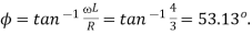 The maximum possible value of is
  .
.
Firing angle control range is 
(b) the maximum value of rms load current  occurs when
  . But at this value of firing angle, the power circuit of ac voltage controller behaves as if load is directly connected to ac source. Therefore, maximum value of rms load current is
(c)Maximum Power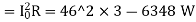
Power factor =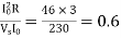
(d) Average thyristor current is maximum when = and conduction angle =π
(e) Maximum value of  occurs when
Its value is maximum when 
 A/sec
A/sec
(f) For  , the conduction angle is
  For
For  , and
, and  gives a conduction angle of about
Q4) For the circuit shows is in fig. (a) sketch the waveforms of output voltage and current for the following values of firing angles.
(a) Only T2 is triggered at t=0, 2π, 4π etc.
(b) Only T1 is triggered at t=0, 2π, 4π etc.
(c) T2 is triggered at t=0, 2π, 4π etc. but T1 is triggered at t=, 2π+, 4π+ and so on. Take around 
A4)
(a) At =0 supply voltage is passing through zero and becoming positive. Therefore, when thyristor T2 is triggered at t=0, 2π, 4π etc. it gets turned on and load voltage
  equals source voltage
  At π,3π etc, as source voltage tends to become negative, T2 is turned off as load current
  is zero. Load voltage
  from π to 2π etc as shown in fig (b-i). For R load, current waveform is identical with voltage waveform.
(b) This part is similar to part(a), except that the voltage amplitude is now  volts fig (b-ii).
(c) At t=0, 2π, 4π etc. when T2 is triggered it gets turned on and 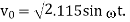 At t=, 2π+, 4π+ etc. when forward biased thyristor T1 is triggered, it gets turned on. But when T1 gets on, voltage equal to
  appears as reverse bias across T2, it is therefore turned off at t=, 2π+, 4π+ etc. when forward biased thyristor T1 is triggerd, it gets turned bias across T2, it is therefore turned off at t=, 2π+ etc. thus, from t=0 to
  follows the curve
  but from t= to π follwos the curve
  as shown in fig.
(b-iii) from π to 2π,  From 2π to 2π+,
 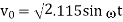 and from 2π+ to 3 π,
  . As the load resistive, load current waveform is identical with load voltage waveform.
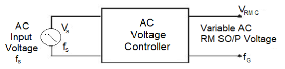
- AC voltage regulators have a constant voltage ac supply input and incorporate semiconductor switches which vary the rms voltage impressed across the ac load. These regulators fall into the category of naturally commutating converters since their thyristor switches are commutated by the alternating supply. This converter turn-off process is termed line commutation.
- The regulator output current, hence supply current, may be discontinuous or non-sinusoidal and therefore input power factor correction and harmonic reduction are usually necessary, particularly at low output voltage levels.
- Therefore, ac to ac converters are potentially more efficient but usually involve a larger number of switching devices and output is lost if the input supply is temporarily lost.
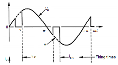
Single-phase ac regulator
AC voltage regulator is a type of thyristor power converter which is used to convert a fixed voltage, fixed frequency ac input supply to obtain a variable voltage ac output. The RMS value of the ac output voltage and the ac power flow to the load is controlled by varying (adjusting) the trigger angle ‘α’
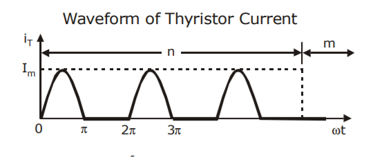
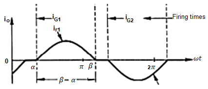
The basic principle of on-off control technique is explained with reference to a single phase full wave ac voltage controller circuit shown below. The thyristor switches T1 and T2 are turned on by applying appropriate gate trigger pulses to connect the input ac supply to the load for ‘n’ number of input cycles during the time interval ON t .
The 3 thyristor switches T1 and T2 are turned off by blocking the gate trigger pulses for ‘m’ number of input cycles during the time interval OFF t . The ac controller ON time ON t usually consists of an integral number of input cycles.
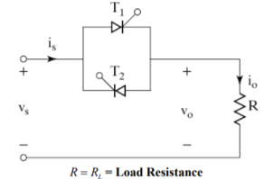
Figure 16. Single phase AC regulator
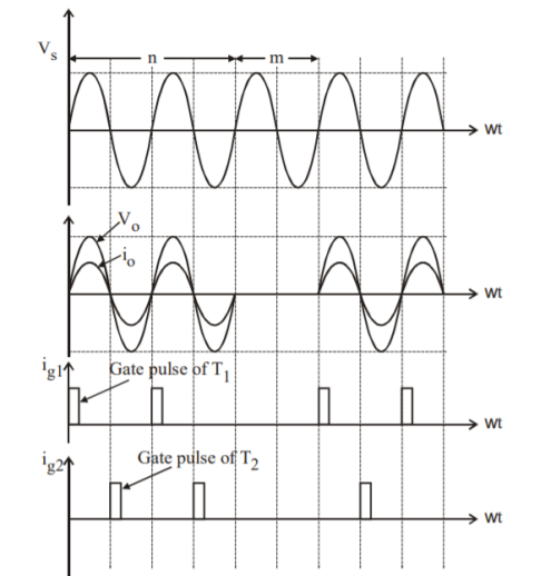
Figure 17. Waveforms
R-L load
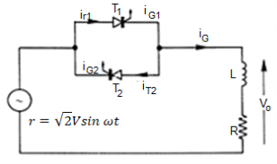
(b)
Figure 18. AC regulator for R-L load
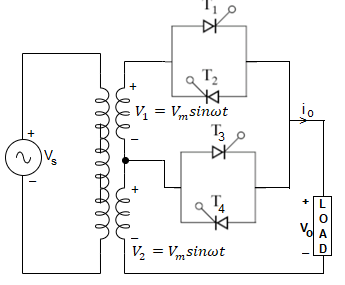
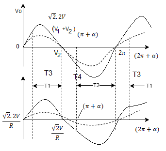
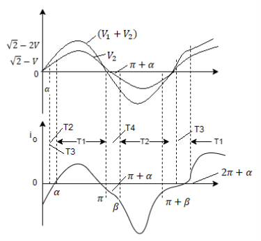
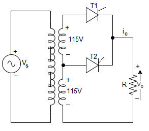
Figure 19. Two stage AC voltage regulator
The two stage sequence control of ac voltage regulators employs two stage in parallel as shown in figure a. The turns ratio from primary to each secondary is taken as unity. This means that for source voltage vs = Vm sinwt, v1=v2 = Vm sin wt and sum of two secondary voltage is 2Vm sin wt.
The load may be R or R-L. For both types loads for obtaining output voltage control from zero to rms value.
Resistance load:
The load current waveform is identical with output voltage waveform. When thyristor pair T3, T4 is in operation the output and voltage and current waveform are shown in figure.
When T3, T4 is in operation then output voltage and current waveforms are shown in (b). When both the pairs T1, T2, T3 and T4 are in operation then firing angle for T3,T4is zero and firing angle α for pair T1, T2 is varied from 180 to zero for obtaining output voltage from V to 2V
R-L load:
When pair T3, T4 in operation then the waveforms of output voltage and current waveform is shown in fig (b)and (c) for α > Ø and α ≤ Ø.
For obtaining output voltage from V to 2V firing angle for T3, T4 is zero for T1, T2 is varied from 180 to zero. For T1, T3 firing pulses vary for wt = 0 to π and during negative half cycle t2, t4 extend from wt = π to 2π
Key takeaway
The two stage sequence control of ac voltage regulators employs two stage in parallel. The turns ratio from primary to each secondary is taken as unity. This means that for source voltage vs = Vm sinwt, v1=v2 = Vm sin wt and sum of two secondary voltage is 2Vm sin wt.
The load may be R or R-L. For both types loads for obtaining output voltage control from zero to rms value.
References:
- Vedam Subramanyam - Power Electronics, New Age International, New Delhi.
- Dubey, Donalda, Joshi, Sinha, Thyristorised Power controllers, Wiley Eastern New Delhi.
- M. D. Singh and K. B. Khandchandani, Power Electronics, Tata McGraw Hill.
- Jai P. Agrawal, Power Electronics systems theory and design LPE, Pearson Education, Asia.
- L. Umanand, Power Electronics – Essentials and Applications Wiley Publication.
- J. Michael Jacob – Power Electronics Principal and Applications.
- M. H. Rashid - Power Electronics Handbook, Butterworth-Heinemann publication, 3rd edition.


