Unit - 3
Single Phase AC-DC Converter
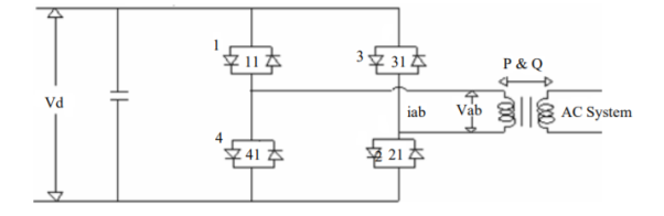
Figure 1(a). Single Phase Full Wave Bridge Converters
- Figure 1 shows a single- phase bridge converter consisting of four valves that is valves (1-1') to (4 -4'), a capacitor to provide stiff D.C.
- Voltage and two A.C. Connection points „a‟ and „b‟. The designated valve numbers represent their sequence of turn on and turn off operation.
- The D.C. Voltage is converted to A.C. Voltage with the appropriate valve turn-off sequence is explained below:
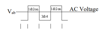
Fig (b)
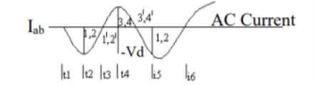
Fig (c)
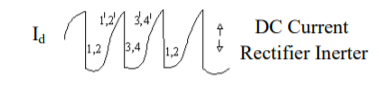
Fig (d)

Fig (e)
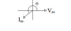
Fig (f)
- In fig (b) when devices 1and 2 are turned on voltage „Vab‟ becomes „+Vd‟ for one half cycle and when devices 3 and 4 turned off „Vab‟ becomes „- Vb‟ for the other half cycle.
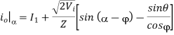
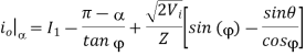
- In fig (c) Suppose the current flow) is A.C. Wave form which is a sinusoidal wave form Iab, the angle θ leads with respect to the square-wave voltage wave form t1 the operation is illustrated.
- From instant t1 to t2 when devices 1 and 2 are ON and 3 and 4 are OFF, „Vab‟ is +ve and Iab is -ve. The current flows through device 1 into A.C. Phase “a‟ and then out of A.C. Phase “b‟ through device “2‟ with power flow from D.C. To A.C. (inverter action).
- From instant t2 to t3 the current reverses that is it becomes +ve and flows through diodes 1' and 2' with power flow from A.C. To D.C. (rectifier action)
- From instant t3 and t4 device 1 and 2 are OFF and 3 and 4 are ON, Vab becomes -ve and Iab is still +ve the current flow through devices 3 and 4 with power flow from D.C. To A.C. (inverter action).
- From instant t4 and t5 devices 3 and 4 still ON and 1 and 2 OFF Vab is -ve current Iab reverses and flows through diodes 3' and 4' with power flow from A.C. To D.C. (rectifier operation)
Fig(d) shows D.C. Current wave form and Fig (e) shows Voltage across valve (1-1') Fig (f) shows phasor of power flow from A.C. To D.C. With lagging power factor.
Four operating modes in one cycle of a single- phase converter is shown in table
ORD | Devices |  |  | Conducting devices | Conversion |
1 | 1&2 ON 3&4 OFF | +ve | -ve | 1 and 2 | Inverter |
2 | 1&2 ON 3&4 OFF | +ve | +ve | 1’ and 2’ | Rectifier |
3 | 1&2 OFF 3&4 ON | -ve | +ve | 3 and 4 | Inverter |
4 | 1&2 OFF 3&4 ON | -ve | -ve | 3’ and 4’ | Rectifier |
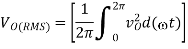
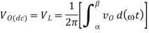
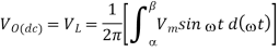
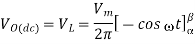
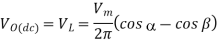
Derivation of output voltage and current
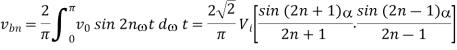
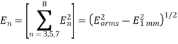
Therefore, the RMS value of the nth harmonic
RMS value of  can of course be completed directly from
Where 
Now at steady state 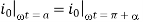 since
since  is periodic over the chosen into boundary condition we obtain
The input current  is related to
  as follows:
 for
for 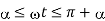
 otherwise
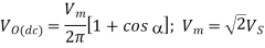
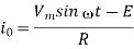
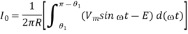
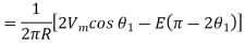
Example
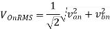
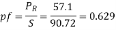
A single-phase half bridge inverter has a resistor load of 2.4 W and the d.c. Input voltage of 48 V. Determine: (i) RMS output voltage at the fundamental frequency (ii) Output power P0 (iii) Average and peak currents of each transistor (iv) Peak blocking voltage of each transistor. (v) Total harmonic distortion and distortion factor. (vi) Harmonic factor and distortion factor at the lowest order harmonic.
Solution:
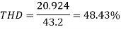
(i) RMS output voltage of fundamental frequency, E1 = 0.9 x 48 = 43.2 V.
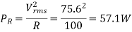
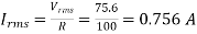
(ii) RMS output voltage, Eorms = E = 48 V. Output power = E 2 /R = (48)2 /2.4 = 960 W
(iii) Peak transistor current = Ip = Ed/R = 48/2.4 = 20 A. Average transistor current = Ip/2 = 10 A. (iv) Peak reverse blocking voltage, VBR = 48 V.
(iv) RMS harmonic voltage
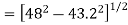

(vii) Lowest order harmonic is the third harmonic RMS value of third harmonic is
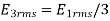
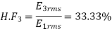
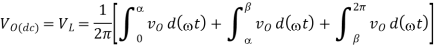
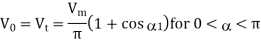
Fig (a) below shows a single-phase half-controlled (semi-converter) rectifier. This configuration consists of a combination of thyristors and diodes and used to eliminate any negative voltage occurrence at the load terminals. This is because the diode Df is always activated (forward biased) whenever the load voltage tends to be negative. For one total period of operation of this circuit, the corresponding waveforms are shown in Fig.(b) below.
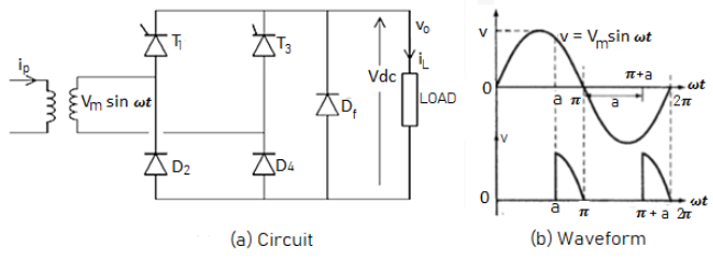
Fig 2 Semi-converter
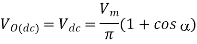
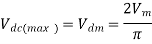
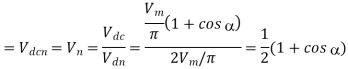
The average value of the load voltage Vdc can be calculated as follows
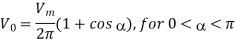
Therefore, the average output voltage can vary from 0 to Vm /π when varying α from π to 0 respectively.
The average value of the load current Idc as follows

The rms value of the load voltage Vrms can be calculated as follows
The diode D2 and D4 conducts for the positive and negative half cycle of the input voltage waveform respectively. On the other hand, T1 starts conduction when it is fired in the positive half cycle of the input voltage waveform and continuous conduction till T3 is fired in the negative half cycle. Figure below shows the circuit diagram and the waveforms of a single phase half controlled converter supplying an R – L – E load.
Key takeaway
The average value of the load current Idc as follows

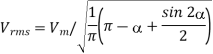
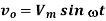
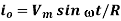
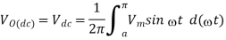
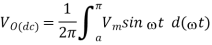
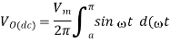
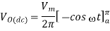
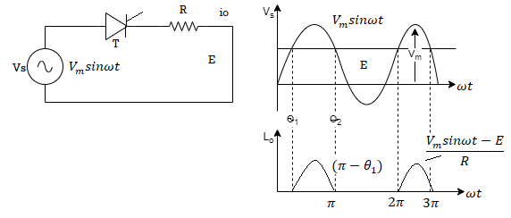
Single Phase Half Wave Controlled Rectifier with pure resistive (R) Load
Figure Shows the circuit diagram of Single Phase Half Wave Controlled Rectifier with Resistive Load. In this Circuit, an SCR (T) is used to rectify the incoming Sine Wave from the Input, and this rectified output will be supplied to a Resistive load.
V0 = Load output voltage
i0 = Load current
VT = Voltage across the Thyristor
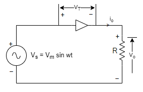
Fig 3 Single phase half wave controlled rectifier
During the Positive Half Cycle of the Input Supply, the SCR (T) is forward biased. The load output voltage is zero till SCR triggered. During this cycle, the SCR is Triggered at a firing angle ωt = α and SCR (T) will Start conducting. But as soon as the supply voltage becomes zero at ωt = π, the load current will become zero
After ωt = π (During Negative Half Cycle), SCR (T) is reversed biased and will Turned OFF at ωt = π and will remain in OFF condition till it is fired again at ωt = (2π+α). The wave shapes for voltage and current in case of Resistive load are shown below:
Fig 4 Waveform
Therefore, the load output voltage and current for one complete cycle of input supply voltage may be written as
 for
for 
 for
for 
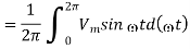
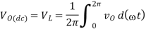
Calculation of Average Load Output Voltage:
As we know that, average value of any function f(x) cab be calculated using the formula
Let us now calculate the average value of output voltage for Single Phase Half Wave Controlled Rectifier.
Average value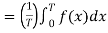
Let us now calculate the average value of output voltage for single phase half wave-controlled rectifier.
Average Value of Load output Voltage

Since the value of load output voltage is zero from  and
and  , therefore
From the expression of average output voltage, it can be seen that, by changing firing angle α, we can change the average output voltage.
The average output voltage is maximum when firing angle is zero and it is
Minimum when firing angle α = π. This is the reason, it is called phase
Controlled rectifier. Average load current for Single Phase Half Wave Controlled Rectifier can easily be calculated by dividing the average load output voltage by load resistance R.
Single Phase Half-Wave Controlled Rectifier with Inductive-Load
Figure Shows (a) the circuit diagram of Single Phase Half Wave Controlled Rectifier with Inductive Load. In this Circuit, an SCR (T) is used to rectify the incoming Sine Wave from the transformer secondary, and this rectified output will be supplied to an inductive load, such as a motor winding or relay coil.
The wave shapes for voltage and current in case of an inductive load are given in Fig. b. The load is assumed to be highly inductive.
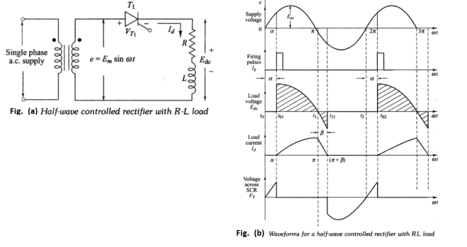
Fig 5 (a) Half wave controlled rectifier (b) Waveform for RL load
During the Positive Half Cycle of the Input Supply, the SCR (T) is forward biased. The load output voltage is zero till SCR triggered. During this cycle, the SCR is Triggered at a firing angle ωt = α and SCR (T) will Start conducting. The SCR will continue conducted in positive half cycle.
During Negative Half Cycle, when the supply voltage reverse, the SCR (T) is kept conducting continuously due to the fact that current through the inductance cannot be reduced to Zero. During negative voltage half-cycle, current will continuously flow till the energy stored in the inductance is dissipated in the load resistor and a part of the energy is fed back to the source.
The effect of inductive load is increased in the conduction period of SCR. Due to this reason, effective Load Voltage and Load Current will reduced. This problem can be resolved by connecting a Free Wheeling Diode in anti- parallel with the inductive Load.
Freewheeling Diode
A freewheeling diode is basically a diode connected across the inductive load terminals to prevent the development of high voltage across the switch. When the inductive circuit is switched off, this diode gives a short circuit path for the flow of inductor decay current and hence dissipation of stored energy in the inductor. This diode is also called Flywheel or Fly-back diode.
Purpose of using Freewheeling Diode:
1. The Freewheeling Diode improves the waveform of the load current of Rectifier
Circuits, inverter circuits, and chopper circuits by making it continuous.
2. The Freewheeling protect the SCRs from damage in the circuits with Inductive Load
From the excessive reverse voltage creating by the Inductive Load.
3. The Freewheeling Diode improves the Input Power Factor of Phase controlled
Rectifiers.
4. The Freewheeling diode sustains the average output voltage of the circuit with
Inductive Load.
5. It also helps to reduce Ripple components in the output signal of the circuit with
Inductive Load.
Single Phase Half-Wave Controlled Rectifier with Inductive load and Freewheeling Diode
Figure Shows the circuit diagram of Single Phase Half Wave Controlled Rectifier with Inductive Load and Free Wheeling Diode. In this Circuit, a SCR is used to rectify the incoming sine wave from the transformer secondary, and this rectified output will be supplied to an inductive load, such as a motor winding or relay coil. The Free Wheeling Diode is connected across the Inductive Load in reverse biasing.
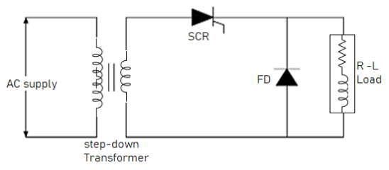
Fig 6 Single Phase Half-Wave Controlled Rectifier with Inductive load and Freewheeling Diode
The wave shapes for voltage and current in case of an inductive load with Freewheeling Diode is shown below:
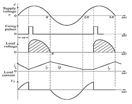
Fig 7 Waveform of half wave-controlled rectifier with inductive load and freewheeling diode
During the Positive Half Cycle of the Input Supply, the SCR is forward biased. The load output voltage is zero till SCR triggered. During this cycle, the SCR is Triggered at a firing angle ωt = α and SCR will Start conducting. The SCR will continue conducted in positive half cycle and allowing the current through Inductive (R-L) Load. The freewheeling diode (FD) is reverse biased During this half-cycle.
During the Negative Half-Cycle, the Freewheeling Diode becomes forward biased and the SCR will Turned OFF, the current that was previously flowing through the SCR and the load inductance, also starts to switch OFF, which causes the inductor to develop a large reverse voltage (positive on the bottom of the inductor, negative on the top) to try and maintain the previous current flow. This large reverse voltage spike would ordinarily be applied across the SCR (positive on the anode, negative on the cathode), potentially forcing it to continue to conduct when the gate is no longer enabled, and potentially damaging the SCR.
For this reason, a freewheeling diode (FD) is connected in parallel with the inductive load. With FD present, the large reverse voltage that would normally develop across the load inductance, causes FD to become forward biased, which acts like a short-circuit to clamp the reverse voltage spike that would otherwise occur to a safe level, corresponding to the forward voltage drop across FD and output voltage across the load will Zero during this Negative Half Cycle and current will flow continuously as shown in voltage & Current Wave shapes.
Single Phase Full Wave Half Controlled Rectifier with Resistive Load:
Single Phase Full Wave Half (Semi) Controlled Rectifier is a rectifier that convert the AC voltage into DC voltage during both the positive and Negative half cycles.
In Half Controlled Rectifier, One SCR and one Diode conducts for positive half cycle and other one SCR and other Diode conducts for negative half cycle to convert the AC voltage to DC voltage.
The Circuit Diagram Full Wave Half controlled rectifier is as shown below:
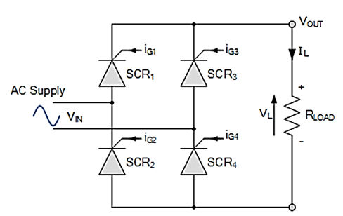
Fig 8 Circuit for Full wave rectifier with R load
During the Positive Half Cycle of the Input VIN Signal, The Current flowing through the path of: Upper Terminal of the Supply (+), SCR1, Load (RL), D2, and back to Lower Terminal (-) of the Supply.
Similarly, During the Negative Half Cycle of Input VIN, The Current flowing through the path of: Lower Terminal (+), SCR2, Load (RL), D1 and back to Upper Terminal -) of the Supply.
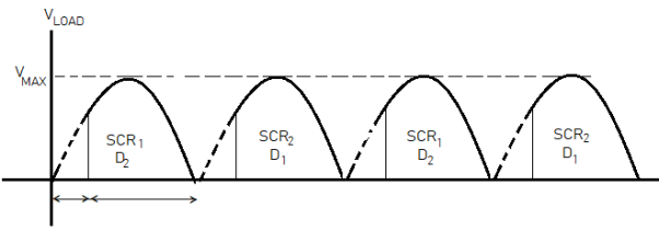
Fig 9 Waveform
It is clear that one SCR from the top group (SCR1 or SCR2) and its corresponding Diode from the bottom group (D2 or D1) must conduct together for any load current to flow.
Thus, the average output voltage, VAVE is dependent on the Firing Angle α for the two SCRs included in the Half-Controlled Rectifier as the two diodes are uncontrolled and pass current whenever forward biased. So, for any gate firing angle α, the average output voltage is given by:
Vave = (Vmax/π) cosα
Iave= Vave/RL
Full Wave Fully-controlled Bridge Rectifier With R-L Load
In the Full Wave Fully-Controlled Rectifier Configuration, the average DC load voltage is controlled using two thyristors / SCRs per half-cycle. Thyristors T1 and T2 are fired together as a pair during the positive half-cycle, while thyristors T3 and T4 are also fired together as a pair during the negative half-cycle (i.e., 180oafter T1 and T2).
When the load is Inductive, the Output Voltage can be Negative for part of the cycle. This is because an inductor stores energy in its magnetic field which is later released. The Circuit Diagram Full Wave Full controlled rectifier with R-L Load is as shown below
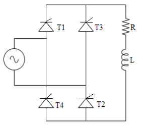
Fig 10 Circuit for full wave fully controlled rectifier with RL load
Operation of this mode can be divided between four modes
Mode 1 (α to π)
In positive half cycle of applied ac signal, SCR's T1 & T2 are forward biased & can be turned on at an angle α. Load voltage is equal to positive instantaneous AC supply voltage. The load current is positive, ripple free, constant and equal to Io. Due to positive polarity of load voltage & load current, load inductance will store energy.
Mode 2 (π to π + α)
At wt = π, input supply is equal to zero & after π it becomes negative. But inductance opposes any change through it. In order to maintain a constant load current & also in same direction. A self-induced emf appears across 'L' as shown. Due to this induced voltage, SCR's T1 & T2 are forward biased in spite the negative supply voltage. The load voltage is negative & equal to instantaneous ac supply voltage whereas load current is positive. Thus, load acts as source & stored energy in inductance is returned back to the ac supply.
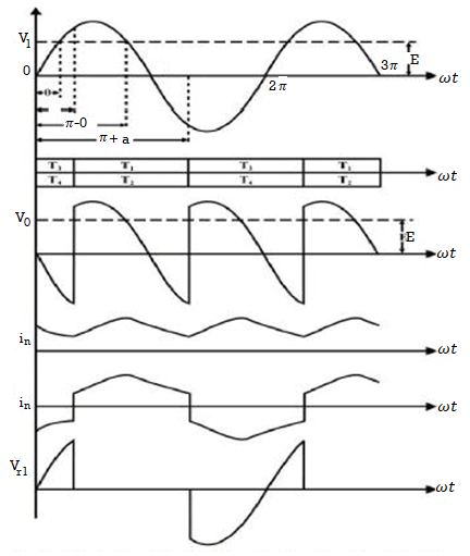
Fig 11 Waveform
Mode 3 (π + α to 2π)
At wt = π + α, SCR's T3 & T4 are turned on & T1, T2 are reversed bias. Thus, process of conduction is transferred from T1, T2 to T3, T4. Load voltage again becomes positive & energy is stored in inductor T3, T4 conduct in negative half cycle from (π + α) to 2 π. With positive load voltage & load current energy gets stored.
Mode 4 (2 π to 2 π + α)
At wt = 2π, input voltage passes through zero. Inductive load will try to oppose any change in current if in order to maintain load current constant & in the same direction. Induced e. m. f. Is Positive & maintains conducting SCR's T3 & T4 with reverse polarity also.
Thus, VL is negative & equal to instantaneous AC supply voltage. Whereas load current continues to be positive. Thus, load acts as source & stored energy in inductance is returned back to ac supply. At wt = α or 2 π + α, T3 & T4 are commutated and T1, T2 are turned ON.
Full Wave Fully-controlled Bridge Rectifier With R-L Load & Free Wheeling Diode:
In the Full Wave fully-controlled rectifier configuration, the average DC load voltage is controlled using two thyristors / SCRs per half-cycle. Thyristors Q1 and Q4 are fired together as a pair during the positive half-cycle, While, thyristors Q2 and Q3 are also fired together as a pair during the negative half-cycle (i.e., 180oafter Q1 and Q4).
When the load is inductive, the output voltage can be negative for part of the cycle. This is because an inductor stores energy in its magnetic field which is later released. A free-wheeling diode can be placed in the circuit to prevent the output voltage from going negative. The Circuit Diagram Full Wave Full controlled rectifier with R-L Load & Free Wheeling Diode is as shown below:
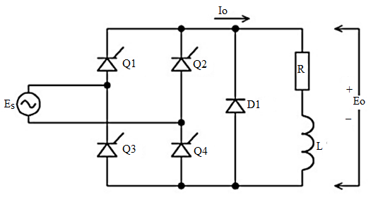
Fig 12 Full Wave Fully-controlled Bridge Rectifier With R-L Load & Free Wheeling Diode
When the load is inductive, the output voltage can be negative for part of the cycle. This is because an inductor stores energy in its magnetic field which is later released. Current continues to flow, and the same thyristors continue to conduct, until all the stored energy is released. Since this occurs sometime after the AC source voltage passes through zero, the output voltage becomes negative for part of cycle.
The negative part of the output voltage waveform reduces the average output voltage E0. A free-wheeling diode can be placed in the circuit to prevent the output voltage from going negative. When the output voltage begins to go negative, the free-wheeling diode conducts.
This maintains the output voltage at approximately zero while the energy stored in the inductor is released. The output voltage waveform is the same as for a purely resistive load, and the average output voltage is therefore greater than it would be without the free-wheeling diode. The addition of a free-wheeling diode makes the output current waveform smoother.
Key takeaway
1. The Freewheeling Diode improves the waveform of the load current of Rectifier
Circuits, inverter circuits, and chopper circuits by making it continuous.
2. The Freewheeling protect the SCRs from damage in the circuits with Inductive Load
From the excessive reverse voltage creating by the Inductive Load.
3. The Freewheeling Diode improves the Input Power Factor of Phase controlled
Rectifiers.
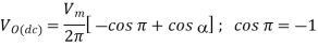
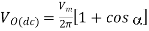
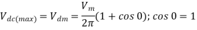
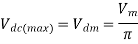
Single Phase Half-Wave Thyristor Converter with a Resistive Load
Expression for the Average (DC) Output Voltage across the Load
 for t= to π
 ;
; 
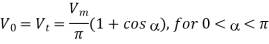
Maximum average (dc) o/p voltage is obtained when 0 and the maximum dc output voltage
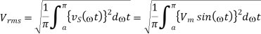
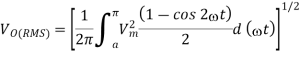
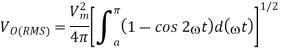
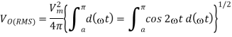
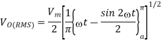
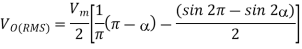
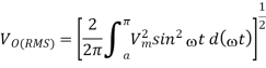
Expression for the RMS Value of Output Voltage of a Single Phase Half Wave Controlled Rectifier with Resistive Load
The RMS output voltage is given by
Output voltage 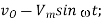 for
for  to π
to π
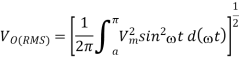
By substituting 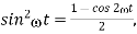 we get
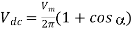
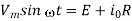
Expression for Average (DC) Load Voltage of a Single Half Wave Controlled Rectifier with RL Load
 for t=0 to and for t= to 2π

The DC Output Voltage and RMS voltage of A Single Phase Semi Converter with R, L, & E Load & FWD
 can be varied from a max value of
  to 0 by varying from 0 to π
For =0, the max. Dc o/p voltage obtained is
Normalized dc o/p voltage is
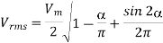
(ii) RMS O/P Voltage 
Semi-converter
The output voltage for half the input cycle will be
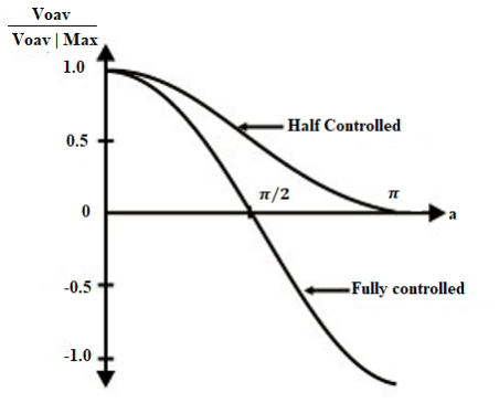
Fig 13 Variation of output voltage as function of firing angle
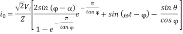
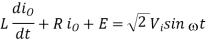
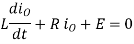
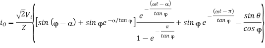
Clearly in addition to the average component, the output voltage (and current) contains a large number of harmonic components. The minimum harmonic voltage frequency is twice the input supply frequency. Magnitude of the harmonic voltages can be found by Fourier series analysis of the load voltage and is left as an exercise. The Fourier series representation of the load current can be obtained from the load voltage by applying superposition principle in the same way as in the case of a fully controlled converter. However, the closed form expression of io can be found as
In the period 
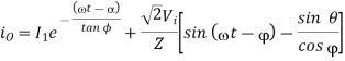
Where 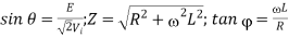
In the period π
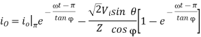
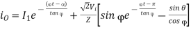
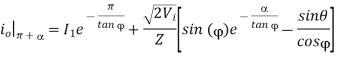
Due to periodic operation
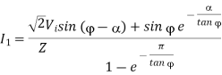
For 
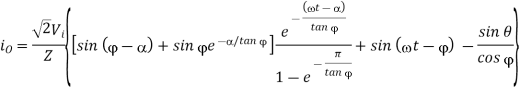
For 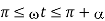
The input current ii is given by
ii = i0 for α ω≤ ≤t π
ii = - i0 for π + α ≤ ωt ≤ 2π
ii = 0 otherwise
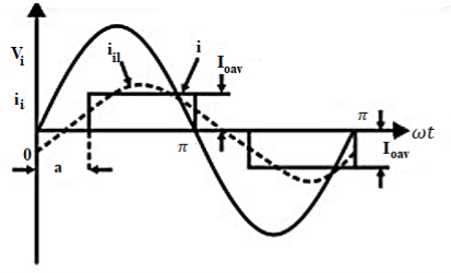
Fig 14 Input current of half controlled converter
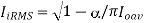
The displacement factor 
Distortion factor 
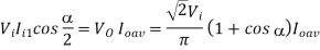
Power factor =displacement factor × distortion factor
The input power factor is defined as the ratio of the total mean input power to the total RMS input volt-amperes.
PF = (V1 I1 cos φ1) / (Vrms Irms)
Where V1 = phase voltage
I1 = fundamental component of the supply current
φ1 = input displacement angle
Irms = supply rms current.
Total Harmonic Distortion Factor is a measure of the distortion in the output waveform.
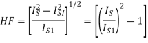
Where:
Is = RMS value of input supply current.
Is1 = RMS value of fundamental component of the input supply
Transformer Utilization Factor (TUF) is given as
TUF = Po(dc)/Vs x Is
Where:
VS = RMS value of transformer secondary output voltage (RMS supply voltage at the secondary).
Is = RMS value of transformer secondary current (RMS line or supply current).
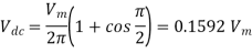
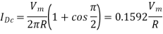
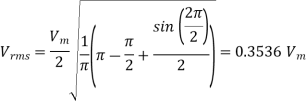
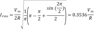
Q1) The single-phase half wave rectifier has a purely resistive load of R and the delay angle is α=π/2, determine: 𝑉𝑑𝑐, 𝐼𝑑𝑐, 𝑉𝑟𝑚𝑠, 𝐼𝑟𝑚𝑠.
A1)
Q2) Design a circuit to produce an average voltage of 40V across a 100Ω load resistor from a 120Vrms 60-Hz ac source. Determine the power absorbed by the resistance and the power factor.
A2)
 so
so 

Q3) For the circuit of controlled half-wave rectifier with RL Load, the source is 120Vrms at 60 Hz, R=20Ω, L=0.04H, and the delay angle is 45o. Determine (a) an expression for i(𝜔t), (b) the rms current, (c) the power absorbed by the load, and (d) the power factor.
A3)
(a) 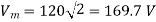

 for
for 
(b)
(c) 
(d) 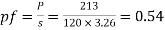
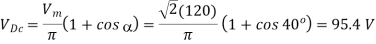
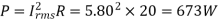
Q4) The full-wave controlled bridge rectifier has an ac input of 120Vrms at 60 Hz and a 20Ω load resistor. The delay angle is 40o. Determine the average current in the load, the power absorbed by the load, and the source voltamperes.
A4)

The rms current in the source is also 5.80 A, and the apparaent power of the source is
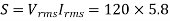 =696 VA
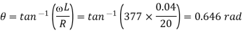
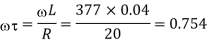
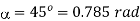
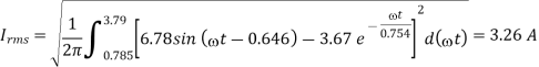
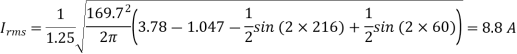
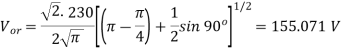
Q5) A controlled full-wave bridge rectifier has a source of 120Vrms at 60Hz, R=10Ω, L=20mH, and α=60o. Determine (a) an expression for load current, (b) the average load current, and (c) the power absorbed by the load.
A5)
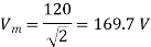

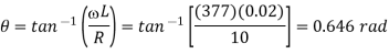
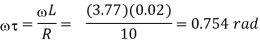
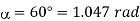
(a) 
Solving  numerically for , =3.78 rad(216
 ), Sinceπ+=4/29>, the current is discontinuous and the above expression for current is valid.
(b) 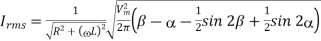
(d) 
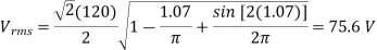
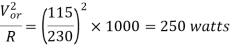
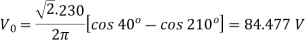
Q6) A single phase 230V, 1kW heater is connected across 1-phase 230V, 50Hz supply through an SCR. For firing angle delay of 450 and 900, calculate the power absorbed in the heater element?
A6)
Heater resistance R
The value of rms voltage for =45° is
Power absorbed by heater element for =45° is
For =90° rms voltage is
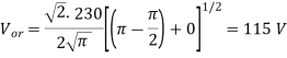
Power absorbed =90° is
Q7) A dc battery is charged through a resistor R as shown in fig.
(a) Derive on expression for the average value of charging current in terms of  etc. On the assumption that SCR is fired continuously.
(a) For an ac source voltage of 230 V, 50 Hz, find the value of average charging current for R=8 and E=150 V.
(b) Find the power supplied to battery and that dissipated in the resistor.
(c) Calculated the supply pf
A7)
For the circuit of the voltage equation is
It seen from fig. That SCR is turned on when  and is turnedoff when
  , where
  . The battery charging requires only the average current
 given by
(a) here 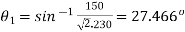
(b) Power supplied to battery
For finding the power dissipated in R, rms value of charging current must by obtained
Power dissipated in resistor = watts
watts
(c) supply pf=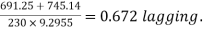
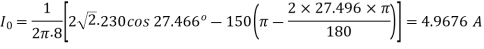
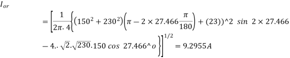
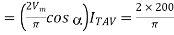
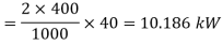
Q8) A 230 V, 50 Hz one-pulses SCR controlled converter is triggered at a firing angle of 40°
And the current extinguishes at angle of 210 °. Find the circuit turn off time, average output voltage and the average load current for
(a) R=5 and L=2mH
(b) R=5 L=2mH and E=110V
A8)
(a) Circuit turn off time 
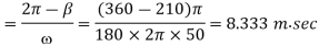
Average output voltage
Average load current 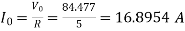
(b) Fig. Shows that circuit turn-off time is again 8.333 msec average load current

Average load voltage
Q9) SCRs with peak forward voltage rating of 1000V and average on-state current rating of 40A are used in single-phase mid-point converter and single-phase bridge converter. Find the power that these two converters can handle. Use a factor of safety of 2.5
A9)
Maximum voltage across SCR in single-phase mid-point converter is  , therefore, this coverter can be designed for a maximum voltage of
Maximum average power that mid-point converter can handle
 ×40×1/1000 =5.093 kW
SCR in a single-phase bridge converter is subjected to a maximum voltage ,
,
Therefore maximum voltage for which this converter can be designed is

Maximum average power rating of bridge converter
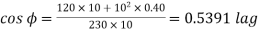
Q10) A single-phase full converter bridge is connected to RLE load. The source voltage is 230 V, 50Hz. The average load current of 10A is continuous over the working range. For R=0.4 and L=2mH, compute
(a) firing angle delay for E=120 V
(b) firing angle delay for E=-120 V
(c) In case output current is assumed constant, find the input pf for both parts (a) and (b)
A10)
For E=120 V the full converter is operating as a controlled rectifier.
 =120+10×0.4=124V

For  power flows from ac source to dc load.
(b) for  , the full converter is operating as a line commutated inverter.

For =124 , the power flows from de source to ac load.
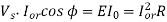
(c) for constant load current, rms value of load current  is
is

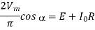
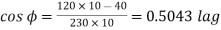
For =53.21
For =124.1
The dual converter comprises of two converters which can perform dual operations. The one can operate as rectifier and other as an inverter. The converters are connected antiparallel to each other. They have same supply as input. Here we can observe four quadrant operations.
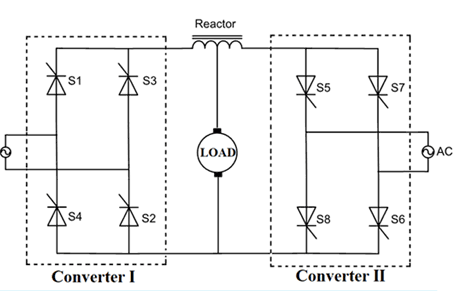
Fig 15 Dual Converter Circuit
The dual converter can operate in two modes-
Circulating Current Mode
- In this case both the converters are ON simultaneously. Hence, there is circulating current is present.
- The firing angles of the two converters is such that α1 + α2 =1800
- For the firing angle 0< α1<900 converter 1 acts as a controlled rectifier.
- For the firing angle 900< α2<1800 converter 2 acts as an inverter. The value of voltage Vdc and Idc both are positive.
- For the firing angle 900< α1<1800 converter 1 acts as an inverter.
- For the firing angle 0< α2<900 converter 2 acts as a controlled rectifier. The value of voltage Vdc and Idc both are negative.
Non- Circulating Current Mode
- There is no circulating current present here between the two converters because one converter acts at one time.
- For the firing angle 0< α1<900 converter 1, the value of voltage Vdc and Idc both are positive.
- For the firing angle 900< α2<1800 converter 2, the value of voltage Vdc and Idc both are negative.
Single Phase Dual Converter
When converters are operating in non-circulating mode with supply source of single phase. When input is applied to first converter is converts AC-DC (rectification). This is transferred to load after filtering. The DC from converter 1 is input to the converter 2 which acts as an inverter and generates AC as final output.
Key takeaway
The dual converter comprises of two converters which can perform dual operations. The one can operate as rectifier and other as an inverter. The converters are connected antiparallel to each other. They have same supply as input.
DC motors are widely used in industry because of its low cost, less complex control structure and wide range of speed and torque. There are many methods of speed control of DC drives namely field control, armature voltage control and armature resistance control methods. DC motors provide high starting torque which is required for traction applications. In DC motor control over a large speed range, both below and above the rated speed can be achieved quite easily. DC motors have inherent disadvantages that it needs regular maintenance and it is bulky in size. DC motors are tailor made, so it is very difficult to replace them. In general, armature voltage control method is widely used to control the DC drives. In this method, a controlled rectifier, or chopper is used but due involvement of power electronics elements, nonlinear torque speed characteristics are observed which are undesirable for control performance.
The torque is produced as a result of interaction of field flux with current in armature conductors and is given by
T m= Kt ɸi
Here Kt is a constant depending on motor windings and geometry and ɸ is the flux per pole due to the field winding. The direction of the torque produced depends on the direction of armature current. When armature rotates, the flux linking the armature winding will vary with time and therefore according to Faraday’s law, an emf will be induced across the winding. This generated emf, known as the back emf, depends on speed of rotation as well as on the flux produced by the field and given by

By applying KVL at input side of in figure
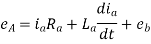
In steady state condtion, 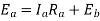
In terms of torque and speed the steady state equation will be given by
So 
Thus, from the above equation it is clear that speed can be controlled by varying there parameters.
The three methods of speed control are as following:
- Armature voltage controlled (Ea).
- Armature resistance controlled (Ra).
- Flux controlled (ɸ)
A separately excited DC motor fed through single phase half wave converter is shown in figure below. Single phase half wave converter feeding a DC motor offers only one quadrant drive. Such type of drives is used up to about 0.5 kW DC motor.
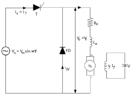
Fig 16 Single phase half wave converter drive
For single phase half wave converter, average output voltage of converter can be calculated as, given as
A half wave converter in the field circuit will increase the magnetic losses of the motor due to high ripple content on the field excitation current, so an ideal DC source is preferred over half wave converter for field circuit. A separately excited DC motor fed through single phase semi-converter is shown in figure below. This converter also offers only one quadrant drive and is used up to 15 kW DC drives.
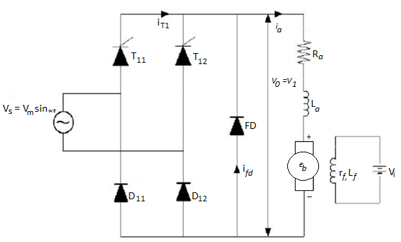
Fig 17 Single Phase Semi-Converter Drive
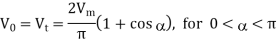
With a single phase semi-converter in the armature circuit, equation gives the average armature voltage as
The armature voltage is varied by single phase full wave converter as shown in figure below. It is a two-quadrant drive, and is limited to applications up to 15kW. The armature converter gives +Vo or –Vo and allows operation in the first and fourth quadrant. The converter in the field circuit could be semi, full or even dual converter. The reversal of the armature or field voltage allows operation in the second and third quadrant.
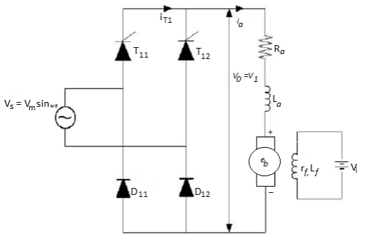
Fig 18 Single Phase Full Converter Drive
The average armature voltage in armature circuit for single phase full converter drive is given by
To realize single phase dual converter, two single phase full converters are connected as shown in figure below
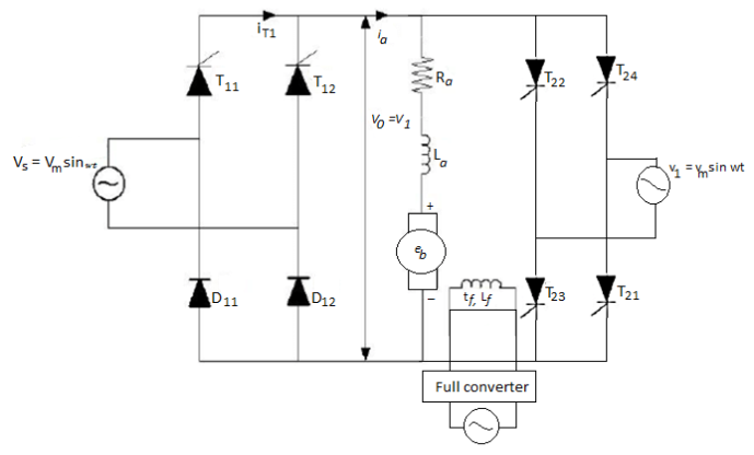
Fig 19 Single phase dual converter drive
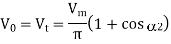
In fig, there are two single phase full wave converters either converter 1 operates to supply a positive armature voltage Vo, or converter 2 operates to supply negative armature voltage –Vo. Converter 1 provides operation in first and fourth quadrants, and converter 2 provides operation in second and third quadrants. It is four quadrant drive and provides four modes of operation: forward powering, forward braking (regeneration), reverse powering, and reverse breaking (regeneration). The field converter could be a full wave converter, a semi converter, or a dual converter. If converter 1 operates at a firing angle of α1 then equation gives the armature voltage as
And similarly, if converter 2 operates at a firing angle of α2 then equation gives the armature voltage as
References:
- Vedam Subramanyam - Power Electronics, New Age International, New Delhi.
- Dubey, Donalda, Joshi, Sinha, Thyristorised Power controllers, Wiley Eastern New Delhi.
- M. D. Singh and K. B. Khandchandani, Power Electronics, Tata McGraw Hill.
- Jai P. Agrawal, Power Electronics systems theory and design LPE, Pearson Education, Asia.
- L. Umanand, Power Electronics – Essentials and Applications Wiley Publication.
- J. Michael Jacob – Power Electronics Principal and Applications.
- M. H. Rashid - Power Electronics Handbook, Butterworth-Heinemann publication, 3rd edition
- S. Li and R. Challo, “Restructuring an electric machinery course with an integrative approach and computer-assisted teaching methodology,”IEEE Transactions on Education., vol. 49,pp. 16-28 Feb.2006.


