Unit - 2
Transistor based Devices and DC-DC converter
The MOSFET transistor is a semiconductor device which is widely used for switching and amplifying electronic signals in the electronic devices.
The MOSFET is a four-terminal device with source(S), gate (G), drain (D) and body (B) terminals. The body of the MOSFET is frequently connected to the source terminal making it a three- terminal device like field effect transistor.

Figure 1. MOSFET
The MOSFET works by varying the width of a channel along which charge carriers flow (electrons or holes). The charge carriers enter the channel at source and exit via the drain.
The width of the channel is controlled by the voltage on an electrode is called gate which is located between source and drain. It is insulated from the channel near an extremely thin layer of metal oxide.
The MOS capacity present in the device is primary.
The MOSFET can function in two ways
- Depletion Mode
- Enhancement Mode
Depletion Mode:

Figure 2. Depletion mode
When there is no voltage on the gate, the channel displays maximum conductance. As the voltage on the gate is either positive or negative, the channel conductivity decreases.
Enhancement Mode
When there is no voltage on the gate the device does not conduct. More is the voltage on the gate, the better the device can conduct.
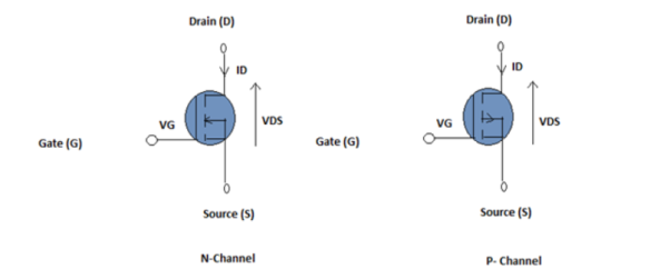
Figure 3. Enhancement mode
Working:
- The working of MOSFET depends upon the MOS capacitor. The MOS capacitor forms main part of MOSFET. The semiconductor surface at the below oxide layer is located between the source and drain terminal
- It can be inverted from p-type to n-type by applying a positive or negative gate voltage respectively. When we apply the positive gate voltage the holes present under the oxide layer with a repulsive force and holes are pushed downward with the substrate.
- The depletion region populated by the bound negative charges which are associated with the acceptor atoms. The electrons reach channel is formed.
- The positive voltage also attracts electrons from the n+ source and drain regions into the channel.
- Now, if a voltage is applied between the drain and source, the current flows freely between the source and drain and the gate voltage controls the electrons in the channel. Instead of positive voltage if we apply negative voltage, a hole channel will be formed under the oxide layer.
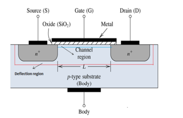
Figure 4. MOSFET construction
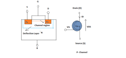
P-channel MOSFET
- The P- Channel MOSFET has a P- Channel region between source and drain. It is a four terminal device such as gate, drain, source, body. The drain and source are heavily doped p+ region and the body or substrate is n-type.
- The flow of current is positively charged holes. When we apply the negative gate voltage, the electrons present under the oxide layer are pushed downward into the substrate with a repulsive force.
- The depletion region populated by the bound positive charges which are associated with the donor atoms. The negative gate voltage also attracts holes from p+ source and drain region into the channel region.
Enhanced mode

Depletion mode
Figure 5. P-channel MOSFET
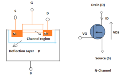
N- Channel MOSFET:
- The N-Channel MOSFET has a N- channel region between source and drain It is a four terminal device such as gate, drain, source, body. This type of MOSFET the drain and source are heavily doped n+ region and the substrate or body is P- type. The current flows due to the negatively charged electrons.
- When we apply the positive gate voltage the holes present under the oxide layer pushed downward into the substrate with a repulsive force. The depletion region is populated by the bound negative charges which are associated with the acceptor atoms. The electrons reach channel is formed.
- The positive voltage also attracts electrons from the n+ source and drain regions into the channel. Now, if a voltage is applied between the drain and source the current flows freely between the source and drain and the gate voltage controls the electrons in the channel.
- Instead of positive voltage if we apply negative voltage a hole channel will be formed under the oxide layer.
Enhancement mode

Depletion mode
Figure 6. N-channel MOSFET
Key takeaway
- The channel width of the MOSFET varies with the flow of the charge carriers and this is the phenomenon behind its working.
- Through the source terminal the carriers enter the channel and flow towards the drain.
- The gate terminal controls the channel width.
- It is insulated from the channel near an extremely thin layer of metal oxide.
IGBT (Insulated Gate Bipolar Transistor)
It is a three-terminal semiconductor switching device that can be used for fast switching with high efficiency used in many types of electronic devices.
These devices are used in amplifiers for switching/processing complex wave patters with pulse width modulation (PWM).
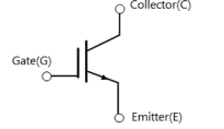
Figure 7. IGBT symbol
IGBT is constructed with equivalent circuit that consists of two transistors and MOSFET.IGBT combines the low saturation voltage of a transistor with the high input impedance and switching speed of a MOSFET. The outcome obtained from this combination delivers the output switching and conduction characteristics of a bipolar transistor, but the voltage is controlled like a MOSFET.

Figure 8. Internal structure
- IGBT has three terminals attached to three different metal layers, the metal layer of the gate terminal is insulated from the semiconductors by a layer of silicon dioxide (SIO2).
- IGBT is constructed with 4 layers of semiconductor sandwiched together. The layer closer to the collector is the p+ substrate layer above that is the n- layer, another p layer is kept closer to the emitter and inside the p layer, we have the n+ layers.
- The junction between the p+ layer and n- layer is called the junction J2 and the junction between the n- layer and the p layer is called the junction J1.

Figure 9. Construction of IGBT
Working:
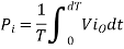
- Consider a voltage source VG connected positively to the Gate terminal with respect to the Emitter. Consider other voltage source VCC connected across The Emitter and the Collector, where Collector is kept positive with respect to the Emitter.
- Due to the voltage source VCC the junction J1 will be forward-biased whereas the junction J2 will be reverse biased. Since J2 is in reverse bias there will not be any current flow inside the IGBT (from collector to emitter).
- Initially, when no voltage applied to the Gate terminal, at this stage the IGBT will be in non-conductive state. As we increase the applied gate voltage, due to the capacitance effect on the SiO2 layer the negative ions will get accumulated on the upper side of the layer and the positive ions will get accumulated on the lower side of the SiO2 layer.
- This will cause the insertion of negative charge carriers in the p region,
- The higher the applied voltage VG greater the insertion of negatively charged carriers. This will lead to a formation of the channel between the J2 junction which allows the flow of current from collector to emitter.
- The flow of current is represented as the current path in the picture, where the applied Gate voltage VG increases the amount of current flow therefore the collector to the emitter also increases.
Types of IGBT
IGBT is classified as two types based on the n+ buffer layer, the IGBTs that are having the n+ buffer layer is called the Punch through IGBT (PT-IGBT), the IGBTs that does not have an n+ buffer layer is called the Non-Punch Through- IGBT (NPT- IGBT).
Punch through IGBT (PT-IGBT) | Non-Punch Through- IGBT (NPT- IGBT) |
These are less rugged in short-circuit failure mode and has less thermal stability | These are more rugged in short circuit failure mode and has more thermal stability. |
The collector is a heavily doped P+layer | The collector is a lightly doped P+layer |
It has a small positive temperature coefficient of ON- State voltage, hence parallel operation requires great care and attention. | The temperature coefficient of ON-state voltage is strongly positive, hence the parallel operation is easy. |
The turn off loss is more temperature-sensitive, hence it increases significantly at a higher temperature. | The turn off a loss is less temperature-sensitive, so, it will remain unchanged with temperature.
|
IGBT Characteristics:
Static Characteristics
BVCES is the collector-emitter voltage at which no more than the specified collector current will flow at the specified temperature. This tracks the actual breakdown voltage.
As shown in Figure, BVCES has a positive temperature coefficient. At a fixed leakage current, an IGBT can block more voltage when hot than when cold.
For the example shown in Figure 8, at -50°C, BVCES is about 93% of the nominal 25°C specification.
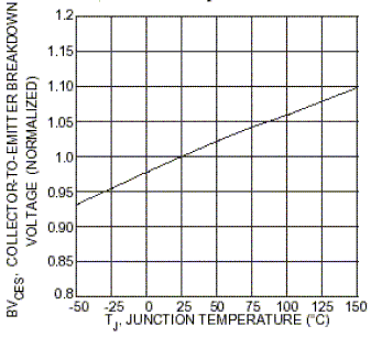
Figure 10. Normalized Breakdown Voltage vs. Junction Temperature
RBVCES — Reverse Collector-Emitter Breakdown Voltage
This is the reverse collector-emitter breakdown voltage specification, i.e., when the emitter voltage is positive with respect to the collector. As with BVCES, RBVCES is the emitter-collector voltage at which no more than the specified emitter current will flow at the specified temperature.
VGE(th) — Gate Threshold Voltage
The gate-source voltage at which collector current begins to flow. Test conditions (collector current, collector-emitter voltage, junction temperature) are also specified. All
MOS gated devices exhibit variation in VGE (th) between devices, which is normal.
VCE(on) — Collector-Emitter on Voltage
This is the collector-emitter voltage across the IGBT at a specified collector current, gate-emitter voltage, and junction temperature. Since VCE(on) is temperature dependent, it is specified both at room temperature and hot.
As current increases, the temperature coefficient of a PT IGBT can actually transition from negative to positive.
ICES — Collector Cut-off Current
This is the leakage current that flows from collector to emitter when the device is off, at a specified collector emitter and gate-emitter voltage. Since leakage current increases with temperature, ICES is specified both at room temperature and hot. Leakage power loss is ICES times collector-emitter voltage.
IGES — gate-emitter leakage current
This is the leakage current that flows through the gate terminal at a specified gate-emitter voltage.
Dynamic characteristics

Figure 11. IGBT Capacitances Cies — Input Capacitance
This is the input capacitance measured between the gate and emitter terminals with the collector shorted to the emitter for AC signals. Cies is made up of the gate to collector capacitance (CGC) in parallel with the gate to emitter capacitance (CGE), or
Cies = CGE + CGC
The input capacitance must be charged to the threshold voltage before the device begins to turn on, and discharged to the plateau voltage before the device begins to turn off. Therefore, the impedance of the drive circuitry and Cies have a direct relationship to the turn on and turn off delays.
Coes — Output capacitance
This is the output capacitance measured between the collector and emitter terminals with the gate shorted to the emitter for AC voltages. Coes is made up of the collector to emitter capacitance (CCE) in parallel with the gate to collector capacitance (CGC), or
Coes = CCE + CGC
For soft switching applications, Coes is important because it can affect the resonance of the circuit.
Cres — Reverse transfer capacitance
This is the reverse transfer capacitance measured between the collector and gate terminals with the emitter connected to ground. The reverse transfer capacitance is equal to the gate to collector capacitance.
Cres = CGC
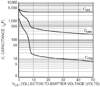
Figure 12 Capacitance vs. Collector-Emitter Voltage
VGEP — Plateau voltage
Figure 11 shows the gate-emitter voltage as a function of gate charge. The turn-on sequence traverses this curve from left to right, turn-off traverses from right to left. The gate plateau voltage VGEP is defined as the gate-emitter voltage when the slope of the gate-emitter voltage first reaches a minimum during the turn-on switching transition for a constant gate current drive condition
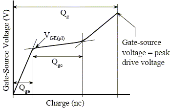
Figure 13 vGE as a Function of Gate Charge Qge,Qgc, and Qg — Gate Charge
Switching characteristics of IGBT:
The IGBT is a Voltage controlled device, hence it only requires a small voltage to the gate to stay in the conduction state. And since these are unidirectional devices, they can only switch current in the forward direction which is from collector to emitter.
A typical switching circuit of IGBT is shown below, the gate volt VG is applied to the gate pin to switch a motor (M) from a supply voltage V+. The resistor Rs is roughly used to limit the current through the motor.
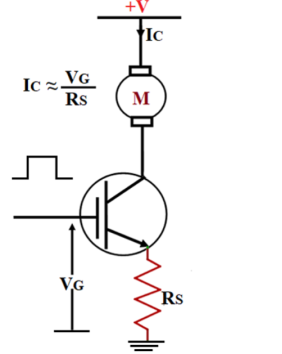
Figure 14. Switching characteristics
The input characteristics of IGBT can be understood from the graph below.
Initially, when no voltage is applied to the gate pin the IGBT is in turn off condition and no current flows through the collector pin. When the voltage applied to the gate pin exceeds the threshold voltage, the IGBT starts conducting and the collector current IG starts to flow between the collector and emitter terminals. The collector current increases with respect to the gate voltage as shown in the graph below.
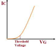
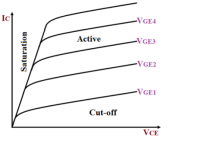
Figure 15. Output characteristics
- The output characteristics of IGBT have three stages,
- Initially, when the Gate Voltage VGE is zero the device is in the off state, this is called the cut-off region.
- When VGE is increased and if it is less than the threshold voltage then there will be a small leakage current flowing through the device, but the device will still be in the cut-off region.
- When the VGE is increased beyond the threshold voltage the device goes into the active region and the current starts flowing through the device. The flow of current will increase with an increase in the voltage VGE as shown in the graph above.
Key takeaways
- IGBTs are used in various applications such as AC and DC motor drives, Unregulated Power Supply (UPS), Switch Mode Power Supplies (SMPS.
- Traction motor control and induction heating, inverters, used to combine an isolated-gate FET for the control input and a bipolar power transistor as a switch in a single device, etc.
Static characteristics:
Drain-source on-state resistance (RDS(ON))
The resistance across drain and source when the MOSFET is in the "on" state.

Figure 16. Static Characteristics
The specified constant drain current, ID, is applied until VGS reaches the specified voltage. At this point, drain-source voltage is measured. On-state resistance is calculated by dividing it by the value of drain current, ID.
Measurement of forward transfer admittance
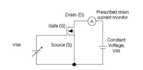
Gate-source voltage, VGS, is increased until drain current, ID, reaches the specified value. Then, VGS is changed only slightly, and the resulting change in drain current, ID, is measured.

Figure 17 Change in VGS w.r.t ID
Dynamic Characteristics
Since power MOSFETs are majority-carrier devices, they are faster and capable of switching at higher frequencies than bipolar transistors.
Switching time measurement circuit and input / output waveform are shown below.

Figure 18. Dynamic Characteristics
td (on): Turn-on delay time
The time from when the gate-source voltage rises above 10% of VGS until the drain-source voltage reaches 90% of VDS
tr: Rise time
The time taken for the drain-source voltage to fall from 90% to 10% of VDS
ton: Turn-on time
The turn-on time is equal to td (on)+ tr.
td (off): Turn-off delay time
The time from when the gate-source voltage drops below 90% of VGS until the drain-source voltage reaches 10% of VDS
tf: Fall time
The time taken for the drain-source voltage to rise from 10% to 90% of VDS
toff: Turn-off time
The turn-off time is equal to td(off)+ tf.
Key takeaways
Features | MOSFET | IGBT |
Drive method | Voltage | Voltage |
Drive circuit | Simple |
|
Input Impedance | High | High |
Drive Power | Low | Low |
Switching Speed | Fast(ns) | Middle |
Operating Frequency | Fast (less than 1MHz) | Middle |
S.O. A | Wide | Wide |
Saturation | Voltage | High |
Principle of operation of chopper
Chopper circuits are known as DC to DC converters. Choppers are used to step up and step down the DC power. They change the fixed DC power to variable DC power. Using these, DC power supplied to the devices can be adjusted to the required amount.

Figure 19. Chopper circuit
The principle of operation of chopper can be understood from the circuit diagram below.
The circuit consists of semiconductor diode, resistor, and load. For all type of chopper circuit, the output voltage value is controlled by periodic closing and opening of the switches used in the circuit.
The chopper can be viewed as an ON/OFF switch that can rapidly connect or disconnect the source to load connection. Continuous DC is given as source to the chopper as Vs and chopped DC is obtained across the load as V0.
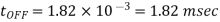
Output Voltage and Current Waveforms
The output voltage and current waveforms of a chopper circuit are shown in figure. From the voltage waveform, it seen that during the period of TON the load voltage V0 is equal to the source voltage Vs.
But when the interval TOFF occurs, the DC voltage step downs to zero, thus making the load short-circuited.

Figure 20. Output Waveform
- In the current waveform, during the interval TON the load current rises to the maximum value. During the interval TOFF, the load current decays.
- In TOFF condition the chopper is off so the load voltage becomes zero.
- But load current flows through the diode FD, making the load short-circuited.
- Thus, the chopped DC voltage is produced at the load.
- The current waveform is continuous which rises during TON state and decays during TOFF state.
Class A Chopper

Figure 21 (a) Class A chopper
Figure shows a Class A Chopper circuit with inductive load and free-wheeling diode. When chopper is ON, supply voltage V is connected across the load that is current i0 flows as shown in figure.
When chopper is OFF, v0 = 0 and the load current continues to flow in the same direction through the free -wheeling diode. Therefore, the average values of output voltage and current are always positive. Hence, Class A Chopper is a first quadrant chopper (or single quadrant chopper).
Figure (b) shows output voltage and current waveforms for a continuous load current.
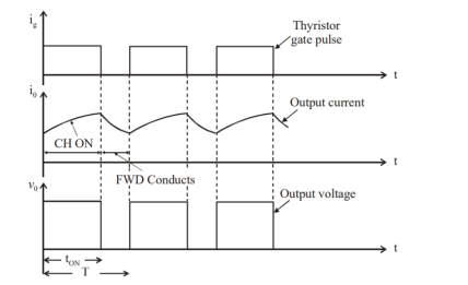
Figure 21 (b) Output voltage and current waveforms.
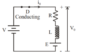
Class A Chopper is a step-down chopper in which power always flows from source to load. It is used to control the speed of dc motor. The output current equations obtained in step down chopper with R-L load can be used to study the performance of Class A Chopper.
CLASS B CHOPPER
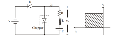
Figure 22 Class B chopper
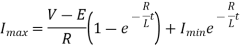
Fig. Shows a Class B Chopper circuit. When chopper is ON, and E drives a current through L and R in a direction opposite to that shown in figure. During the ON period of the chopper, the inductance L stores energy.
When Chopper is OFF, diode D conducts, and part of the energy stored in inductor L is returned to the supply. Also, the current continues to flow from the load to source. Hence the average output voltage is positive and average output current is negative.
Therefore, Class B Chopper operates in second quadrant. In this chopper, power flows from load to source. Class B Chopper is used for regenerative braking of dc motor.
Figure (b) shows the output voltage and current waveforms of a Class B Chopper. The output current equations can be obtained as follows. During the interval diode ‘D’ conducts (chopper is off) voltage equation is given by

For the initial condition i.e., at. The solution of the above equation is obtained along similar lines as in step-down chopper with R-L load
Therefore 
At 


During the interval chopper is ON voltage equation is given by

Redefining the time origin, at t=0, 
The solution for the stated initial condition is


Therefore 

Figure 23. Class B Chopper Output Voltage and current waveform.
CLASS C CHOPPER
Class C Chopper is a combination of Class A and Class B Choppers. Figure a) shows a Class C two quadrant Chopper circuit.
For first quadrant operation, is ON or conducts and for second quadrant operation, is ON or conducts. When is ON, the load current is positive. i.e., flows in the direction as shown in figure
The output voltage is equal to V and the load receives power from the source.
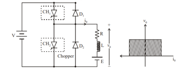
Figure 24. Class C chopper
When CH1 is turned OFF, the energy stored in inductance L forces current to flow through the diode and the output voltage vo=0V, but io continues to flow in positive direction. When CH2 is triggered, the voltage E forces io to flow in opposite direction through L and CH2. The output voltage v0=0.
On turning OFF CH2 the energy stored in the inductance drives current through diode D1 and the supply.
The output voltage v0=V the input current becomes negative and power flows from load to source.
Thus, the average output voltage vo is positive but the average output current io can take both positive and negative values. Choppers CH1 and CH2 should not be turned ON simultaneously as it would result in short circuiting the supply.
Class C Chopper can be used both for dc motor control and regenerative braking of dc motor. Figure shows the output voltage and current waveforms.
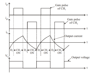
Figure 25. Class C chopper output voltage and current waveform.
Class D chopper
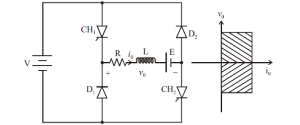
Figure 26. D chopper
Figure shows a class D two quadrant chopper circuit. When both and are triggered simultaneously, the output voltage vo=V and output current Io flows through the load in the direction shown in figure.
When CH1 and CH2 are turned off the load io continues to flow in the same direction through load.
D1 and D2 due to energy stored in inductor L but output voltage vo = -V. The average load voltage vo is positive if chopper ON time (t ON) is more than OFF time t(OFF) and the average output voltage becomes negative if ton<toFF.
Hence, the direction of load current is always positive. But load voltage can be positive or negative.
Output voltage for ton>toff
Output voltage for ton<toff
Figure 27. Output waveforms.
Class E chopper:

Four Quadrant Operation
Figure 28. Class E chopper
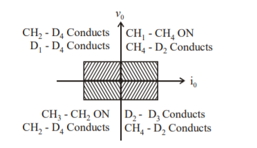
Figure shows a class E 4 quadrant chopper circuit. When they are triggered, output current flows in positive direction as shown in figure through and, with output voltage vo=V. This gives the first quadrant operation.
When both and are OFF, the energy stored in the inductor L drives through and in the same direction, but output voltage vo=-V. Therefore, the chopper operates in the fourth quadrant.
For fourth quadrant operation the direction of battery must be reversed. When Ch2 and Ch3 are triggered, the load current io flows in opposite direction and output voltage vo = -V. Since both io and vo are negative, the chopper operates in third quadrant.
When both CH2 and CH3 are OFF, the load current io continues to flow in the same direction through D1 and D4 and the output voltage vo=V. Therefore, the chopper operates in second quadrant as vo is positive but io is negative. Figure shows the devices which are operative in different quadrants.
Key takeaway
- Class A Chopper is a step-down chopper in which power always flows from source to load. It is used to control the speed of dc motor.
- Therefore, Class B Chopper operates in second quadrant. In this chopper, power flows from load to source. Class B Chopper is used for regenerative braking of dc motor.
- Class C Chopper can be used both for dc motor control and regenerative braking of dc motor. It is the combination of class A and class B chopper.
- Class D chopper can operate in different quadrants.
Solved Examples
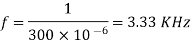
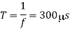
Q1) A Chopper circuit is operating on TRC at a frequency of 2 kHz on a 460 V supply. If the load voltage is 350 volts, calculate the conduction period of the thyristor in each cycle.
A1)

Chopping period 
Output voltage 
Conduction period of thyristor


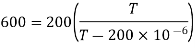
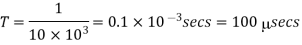
Q2) Input to the step up chopper is 200 V. The output required is 600 V. If the conducting time of thyristor is 200 µsec. Compute – Chopping frequency, – If the pulse width is halved for constant frequency of operation, find the new output voltage.
A2)


Solving for T
T=200s
Chopping frequency 

Pulse width is halved
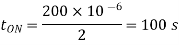
Frequency is constant 

Output voltage 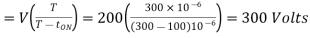
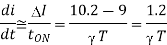
Q3) A dc chopper has a resistive load of 20Ω and input voltage VS = 220V. When chopper is ON, its voltage drop is 1.5 volts and chopping frequency is 10 kHz. If the duty cycle is 80%, determine the average output voltage and the chopper on time.
A3) 

 Voltage drops across chopper =1.5 volts
Average output voltage


 Voltage drops across chopper=1.5 volts
Average Output voltage


Chopper ON time 
Chopping period, 
Chopper ON time


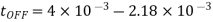
Q4) In a dc chopper, the average load current is 30 Amps, chopping frequency is 250 Hz, supply voltage is 110 volts. Calculate the ON and OFF periods of the chopper if the load resistance is 2 ohms.
A4)


 and
and 

Chopper ON period

Chopper OFF period


CLC:( Current Limit control)
In DC to DC converter the current value varies between maximum and minimum level of constant voltage. In this method the DC to DC converter is turned On and Off to confirm that current is preserved constantly between upper limits and lower limits.
When the current energies beyond the extreme point Dc-Dc converter goes OFF.
When the switch is in its OFF state, current freewheels through the diode and falls in an exponential manner. The chopper is turned ON when the flow of current spreads the minimum level. This technique can be utilized either when the ON time ‘T’ is endless or when the frequency f=1/T.

Current Limit control
Figure 29. Current limit control
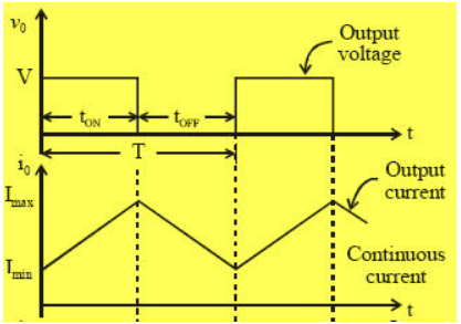
TRC (Time Ratio Control)
In time ratio control the value of the duty ratio, K =TON /T is changed. Here ‘K’ is called the duty cycle. There are two ways to achieve the time ration control, namely variable frequency, and constant frequency operation.
Constant Frequency Operation (PWM technique)
In constant frequency control strategy operation, the ON time TON is changed, keeping the frequency, that is f=1/T, or time period ‘T’ constant. This operation is also named as PWM (pulse width modulation control). Hence, the output voltage can be varied by varying ON time.

Figure 30 Constant Frequency Operation
Variable Frequency Operation (FM technique)
In variable frequency control strategy operation, the frequency (f = 1/T) is changed, then the time period ‘T’ is also changed. This is also named as a frequency modulation control. In both cases, the o/p voltage can be changed with the change in duty ratio.

Figure 31. Variable Frequency Operation
PWM Technique
The input dc voltage is of constant magnitude. The diode rectifier is used to rectify the line voltage. The inverter controls the magnitude and frequency of the ac output voltage. This is achieved by PWM technique of inverter switches and this is called PWM inverters. The sinusoidal PWM technique is one of the PWM technique to shape the output voltage to as close as sinusoidal output.
Basic concepts of switch mode inverter
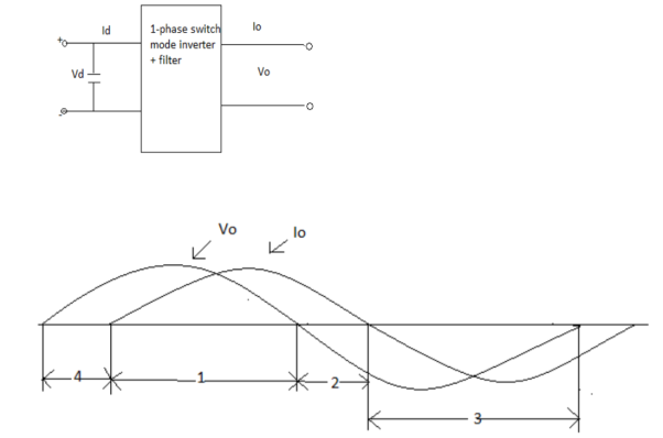

Figure 32 Operation as inverter and rectifier in different quadrants
During interval 1 𝑣0 and 𝑖0 both are positive
During interval 3 𝑣0 and 𝑖0 both are negative
Therefore during 1 and 3 the instantaneous power flow is from dc side to corresponding to inverter mode of operation. In contrast during interval 2 and 4 𝑣0 and 𝑖0 are of opposite sign i.e., power flows from ac side to dc side corresponding to rectifier mode of operation.
Pulse width modulated switching scheme
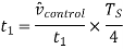
We require the inverter output to be sinusoidal with magnitude and frequency controllable. In order to produce sinusoidal output voltage at desired frequency a sinusoidal control signal at desired frequency is compared with a triangular waveform as show. The frequency of the triangular waveform established the inverter switching frequency. The triangular waveform is called carrier waveform. The triangular waveform establishes switching frequency 𝑓𝑠, which establishes with which the inverter switches are applied. The control signal has frequency 𝑓𝑠 and is used to modulate the switch duty ratio. 𝑓1 is the desired fundamental frequency of the output voltage.
The amplitude modulation ratio 𝑚𝑎 is defined as
ma = Vcontrol/Vtri
The frequency modulation ratio 𝑚f
mf = fs/f1

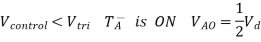
Figure 33 PWM Scheme
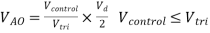
When 

So, the following inferences can be drawn
The peak amplitude of fundamental frequency is  times
times 


Let the Vcontrol vary sinusoidal with frequency f1, which is the desired frequency of the inverter output voltage.
Let Vcontrol=V̂controlsin𝜔1t V̂control ≤ V̂tri


At 
So 


Key takeaway
In DC to DC converter the current value varies between maximum and minimum level of constant voltage. In this method the DC to DC converter is turned On and Off to confirm that current is preserved constantly between upper limits and lower limits.
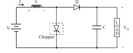
Figure 34. Step Up chopper
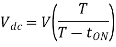
The figure shows Step Up chopper. To obtain load voltage Vo higher than the input voltage V. The values of L and C are chosen depending on the requirement of output voltage.
When the chopper is ON the inductor L is connected across the supply. The inductor current I rises and stores energy during ON time of the chopper tON.
When the chopper is off the inductor current is forced to flow through the diode D and load for a period t OFF. The current tends to decrease resulting in reversing the polarity of induced EMF in L. Therefore, voltage across load is given by

If a large capacitor ‘C’ is connected across the load, then the capacitor will provide a continuous output voltage. Diode D prevents any current flow from capacitor to the source. Step up choppers are used for regenerative braking of dc motors.
Expression for Output Voltage:
Assume the average inductor current to be I during ON and OFF time of Chopper.
When Chopper is ON
Voltage across inductor L=V
Therefore, energy stored in inductor = V.I.ton.
TOn = On period of chopper.
When Chopper is OFF (energy is supplied by inductor to load)
Voltage across L = V0 – V
Energy supplied by inductor L = (Vo-V) I t OFF
Where t OFF = OFF period of chopper.
Neglecting losses, energy stored in inductor L = energy supplied by inductor L
Therefore 


Where T=Chopping period or period of switching


Where  duty cycle
For variation of duty cycle ‘d’ in the range 0<d<1 the output voltage Vo will vary in the range V<Vo<∞.
Problems:
A Chopper circuit is operating on TRC at a frequency of 2 kHz on a 460 V supply. If the load voltage is 350 volts, calculate the conduction period of the thyristor in each cycle.
V = 460 V Vdc = 350V, f=2KHz
Chopping period T = 1/f = 1/ 2 x 10 -3 = 0.5 m sec
Output voltage
Vdc = (tON/T) V
Conduction period of thyristor
TON = T x Vdc / V
TON = 0.5 x 10 -3 x 350 / 460 = 0.38 sec
Input to the step up chopper is 200 V. The output required is 600 V. If the conducting time of thyristor is 200 s sec. Compute Chopping frequency, If the pulse width is halved for constant frequency of operation, find the new output voltage.
Vs = 220V, R = 20 Ω, f = 10KHz.
d = tON/T = 0.80
Vch = voltage drop across chopper = 1.5 Volts
Average output voltage
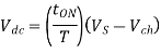
Vdc = (tON/T) (Vs-Vch) = 0.80(220-1.5) = 174.8Volts
Chopper ON time tON = dT
Chopping period T=1/f = 1/10 x 10 3 secs = 100 µsec
Chopper ON time
TON = dT
TOn = 0.80 x 0.1 x 10 -3 = 80 µ sec.
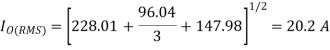
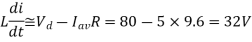
A dc chopper in figure has a resistive load of and input voltage of V = 200 V. When chopper is ON, its voltage drop is 2 V and the chopping frequency is 1 kHz. If the duty cycle is 60%, determine Average output voltage RMS value of output voltage Effective input resistance of chopper efficiency.
V=200V, R=10 , Chopper voltage drop,
  d=0.60, f=1 kHz
Average output voltage

RMS value of output voltage


Effective input resistance of chopper is

 Amps
Amps

Output Power:

Input Power:

Chopper efficiency

Q) A chopper feeding on RL load is shown in figure, with V = 200 V, R = 5, L = 5 mH, f = 1 kHz, d = 0.5 and E = 0 V. Calculate – Maximum and minimum values of load current. – Average value of load current. – RMS load current. – Effective input resistance as seen by source. – RMS chopper current.
A)

V=200V R=5
F=1kHz, d=0.5, E=0
Chopping period is
 secs
secs
Maximum value of load current is given by


Minimum value of load current is given by

Average value of load current is

For linear variation of currents

RMS load current is given by
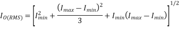

RMS chopper current is given by

Effective input resistance is

 Average source current

Therefore, effective input resistance is

It is a type of DC to DC converter and it has a magnitude of output voltage.
The buck boost converter is equal to the flyback circuit and single inductor is used in the place of the transformer.
There are two types of converters in the buck boost converter that are buck converter and the other one is boost converter. These converters can produce the range of output voltage than the input voltage.
The following diagram shows the basic buck boost converter.
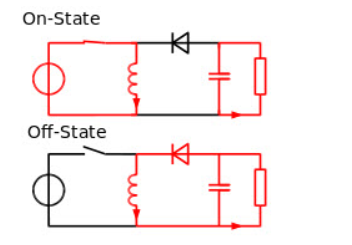
Figure 35 Buck Boost Converter
The working operation of the DC to DC converter is the inductor in the input resistance has the unexpected variation in the input current.
If the switch is ON, then the inductor feeds the energy from the input and it stores the energy of magnetic energy.
If the switch is closed it discharges the energy. The output circuit of the capacitor is assumed as high sufficient than the time constant of an RC circuit is high on the output stage.
The huge time constant is compared with the switching period and make sure that the steady state is a constant output voltage
Vo(t) = Vo(constant) and present at the load terminal.
There are two different types of working principles in the buck boost converter.
- Buck converter.
- Boost converter.
Buck Converter Working
The following diagram shows the working operation of the buck converter. In the buck converter first transistor is turned ON and second transistor is switched OFF due to high square wave frequency.
If the gate terminal of the first transistor is more than the current pass through the magnetic field, charging C, and it supplies the load. The D1 is the Schottky diode and it is turned OFF due to the positive voltage to the cathode.

Figure 36. Buck Converter
The inductor L is the initial source of current. If the first transistor is OFF by using the control unit, then the current flow in the buck operation. The magnetic field of the inductor is collapsed and the back e.m.f is generated collapsing field turn around the polarity of the voltage across the inductor. The current flows in the diode D2, the load and the D1 diode will be turned ON.
The discharge of the inductor L decreases with the help of the current. During the first transistor is in one state the charge of the accumulator in the capacitor. The current flows through the load and during the off period keeping Vout reasonably. Hence it keeps the minimum ripple amplitude and Vout closes to the value of Vs
Boost Converter Working
In this converter the first transistor is switched ON continually and for the second transistor the square wave of high frequency is applied to the gate terminal.
The second transistor is in conducting when the on state and the input current flow from the inductor L through the second transistor.
The negative terminal charging up the magnetic field around the inductor. The D2 diode cannot conduct because the anode is on the potential ground by highly conducting the second transistor.

By charging the capacitor C the load is applied to the entire circuit in the ON State and it can construct earlier oscillator cycles. During the ON period the capacitor C can discharge regularly and the amount of high ripple frequency on the output voltage. The approximate potential difference is given by the equation below.
VS + VL
During the OFF period of second transistor the inductor L is charged and the capacitor C is discharged. The inductor L can produce the back e.m.f and the values are depending up on the rate of change of current of the second transistor switch. The amount of inductance the coil can occupy. Hence the back e.m.f can produce any different voltage through a wide range and determined by the design of the circuit. Hence the polarity of voltage across the inductor L has reversed now.
The input voltage gives the output voltage and atleast equal to or higher than the input voltage. The diode D2 is in forward biased and the current applied to the load current and it recharges the capacitors to VS + VL and it is ready for the second transistor.
Solved Examples
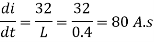
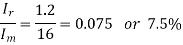
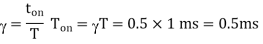
Q1) A transistor dc chopper circuit (Buck converter) is supplied with power form an ideal battery of 100 V. The load voltage waveform consists of rectangular pulses of duration 1 ms in an overall cycle time of 2.5 ms. Calculate, for resistive load of 10 Ω. (a) The duty cycle γ. (b) The average value of the output voltage Vo. (c) The rms value of the output voltage Vorms. (d) The ripple factor RF. (e) The output dc power.
A1)
(a) 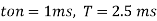

(b) 
(c)
(d) 
(e) 

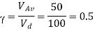
Q2) An 80 V battery supplies RL load through a DC chopper. The load has a freewheeling diode across it is composed of 0.4 H in series with 5Ω resistor. Load current, due to improper selection of frequency of chopping, varies widely between 9A and 10.2. (a) Find the average load voltage, current and the duty cycle of the chopper. (b) What is the operating frequency f? (c) Find the ripple current to maximum current ratio.
A2)
(a) The average load voltage and current are


(b) to find the operating (chopping) frequency
During the ON period

Assume  constant
From eq (1)
But 

Hence 
The maximum current  occurs at =1

Ripple current 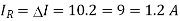
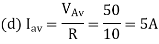
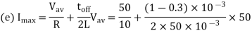
Q3) A DC Buck converter operates at frequency of 1 kHz from 100V DC source supplying a 10 Ω resistive load. The inductive component of the load is 50mH.For output average voltage of 50V volts, find: (a) The duty cycle (b) ton (c) The rms value of the output current (d) The average value of the output current (e) Imax and Imin (f) The input power (g) The peak-to-peak ripple current.
A3)
(a) 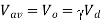
(b) 


(g) 
Batteries are the primary energy-storage devices in ground vehicles. Now days battery fed electric drives are commonly being used for electric vehicles applications, due to various advantages, such as: nearly zero emission, guaranteed load leveling, good transient operation and energy recovery during braking operation. To fulfil these requirements converters with bidirectional power flow capabilities are required to connect the accumulator (battery) to the dc link of the motor drive system.
Battery fed electric vehicles (BFEVs) is required to function in three different modes namely: acceleration mode, normal (steady-state) mode and braking (regenerative) mode. During acceleration and normal modes, the power flow is from battery to motor whereas during braking or regenerative mode the kinetic energy of the motor is converted into electrical energy and fed back to battery.
The DC-DC converter is required to perform mainly two functions: first to match the battery voltage to the motor rated voltage and second to control the power flow under steady-state and transient conditions, so that the drive performance is as per the requirement.
The use of a Bi-directional dc-dc converter for a battery fed electric vehicle drive system. A closed loop speed control technique of the proposed battery fed electric vehicle is designed and implemented using PI controller. The overall drive system reduces the system complexity, cost and size of a purely electric based vehicular system.
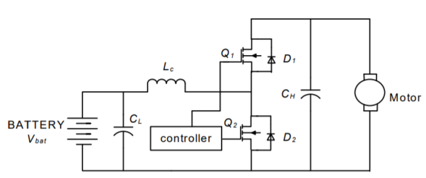
Figure 37 Circuit Diagram
Above figure shows the proposed Bi-directional dc-dc converter fed DC motor drive. In this topology, boost converter operation is achieved by modulating Q2 with the anti-parallel diode D1 serving as the boost mode diode. With the direction of power flow reversed, the topology functions as a buck converter through the modulation of Q1, with the anti-parallel diode D2 serving as the buck-mode diode. It should be noted that the two modes have opposite inductor current directions.
A new control model is developed using PI controller to achieve both motoring and regenerative braking of the motor. A Lithium-ion battery model has been used in this model to verify the motor performance in both motoring and regenerative mode. This controller shows satisfactory result in different driving speed commands.
For the dc–dc converter, the only important part of the inverter–machine subsystem is the zero-sequence impedance and the zero-sequence voltage vz. Thus, the integrated dc–dc converter can be modeled. The time-dependent voltage source vz represents the zero-sequence voltage and vs4 describes the voltage across ss4. These two voltage sources are connected to an LR circuit, modeling the machine’s zero-sequence impedance. Voltage vt represents the transformer voltage.
It has to be mentioned that vz, can only be measured if no zero-sequence current flows; otherwise, it is a theoretical quantity since there is a voltage drop vlr across L0 and R0. The voltage measured between the star point and the negative bus is equal to vz −vlr. This system is similar to a full-bridge rectifier system, but as the voltage vz applied to the system is neither average free (related to the switching frequency) nor free from even harmonics, a conventional modulation scheme cannot be adopted.
In the actual implementation, an active rectifier is used to guarantee that the voltage-time product across the transformer remains below a predetermined level. The described dc– dc con- verter is similar to a dual active bridge. A unidirectional implementation with a diode rectifier would be an-Converter waveforms: zero-sequence voltage vz, voltage vs4 across s4, voltage vt1 across st1, voltage vt2 across st2, and transformer voltage vt. Other possibility, but in order to limit the voltage-time product across the transformer, a special control approach has to be implemented.
Equations
The bi-directional converter is designed based on the input supply voltage and output voltage requirement to drive the electric vehicle at desired speed. The converter power topology is based on a half bridge circuit to control the dc motor. At a given input battery voltage and reference speed command the inductor current has a nearly constant peak to peak swing. The inductor is designed with a specified current ripple of 15A and 20 KHz switching frequency.


References:
- Vedam Subramanyam - Power Electronics, New Age International, New Delhi.
- Dubey, Donalda, Joshi, Sinha, Thyristorised Power controllers, Wiley Eastern New Delhi.
- M. D. Singh and K. B. Khandchandani, Power Electronics, Tata McGraw Hill.
- Jai P. Agrawal, Power Electronics systems theory and design LPE, Pearson Education, Asia.
- L. Umanand, Power Electronics – Essentials and Applications Wiley Publication.
- J. Michael Jacob – Power Electronics Principal and Applications.
- M. H. Rashid - Power Electronics Handbook, Butterworth-Heinemann publication, 3rd edition.
- S. Williamson, M. Lukic, and A. Emadi, “Comprehensive drive train efficiencyanalysisofhybridelectricandfuel cell vehicles based on motor- controller efficiency modeling,” IEEE Trans. Power Electron., vol. 21, no. 3, pp. 730–740, May 2006.
- A. Emadi, S. Williamson, and A. Khaligh, “Power electronics intensive solutions for advanced electric, hybrid electric, and fuel cell vehicular power systems,” IEEE Trans. Power Electron., vol. 21, no. 3, pp. 567– 577, May 2006.
- A. Emadi, M. Ehsani, and J. Miller, “Advanced silicon rich automotive electrical power systems,” in Proc. 18th Digit. Avionics Syst. Conf., St Louis, MO, Oct. 24–29, 1999, vol. 2, pp. 8.B.1-1–8.B.1-8.
Unit - 2
Transistor based Devices and DC-DC converter
The MOSFET transistor is a semiconductor device which is widely used for switching and amplifying electronic signals in the electronic devices.
The MOSFET is a four-terminal device with source(S), gate (G), drain (D) and body (B) terminals. The body of the MOSFET is frequently connected to the source terminal making it a three- terminal device like field effect transistor.
Figure 1. MOSFET
The MOSFET works by varying the width of a channel along which charge carriers flow (electrons or holes). The charge carriers enter the channel at source and exit via the drain.
The width of the channel is controlled by the voltage on an electrode is called gate which is located between source and drain. It is insulated from the channel near an extremely thin layer of metal oxide.
The MOS capacity present in the device is primary.
The MOSFET can function in two ways
- Depletion Mode
- Enhancement Mode
Depletion Mode:
Figure 2. Depletion mode
When there is no voltage on the gate, the channel displays maximum conductance. As the voltage on the gate is either positive or negative, the channel conductivity decreases.
Enhancement Mode
When there is no voltage on the gate the device does not conduct. More is the voltage on the gate, the better the device can conduct.

Figure 3. Enhancement mode
Working:
- The working of MOSFET depends upon the MOS capacitor. The MOS capacitor forms main part of MOSFET. The semiconductor surface at the below oxide layer is located between the source and drain terminal
- It can be inverted from p-type to n-type by applying a positive or negative gate voltage respectively. When we apply the positive gate voltage the holes present under the oxide layer with a repulsive force and holes are pushed downward with the substrate.
- The depletion region populated by the bound negative charges which are associated with the acceptor atoms. The electrons reach channel is formed.
- The positive voltage also attracts electrons from the n+ source and drain regions into the channel.
- Now, if a voltage is applied between the drain and source, the current flows freely between the source and drain and the gate voltage controls the electrons in the channel. Instead of positive voltage if we apply negative voltage, a hole channel will be formed under the oxide layer.

Figure 4. MOSFET construction
P-channel MOSFET
- The P- Channel MOSFET has a P- Channel region between source and drain. It is a four terminal device such as gate, drain, source, body. The drain and source are heavily doped p+ region and the body or substrate is n-type.
- The flow of current is positively charged holes. When we apply the negative gate voltage, the electrons present under the oxide layer are pushed downward into the substrate with a repulsive force.
- The depletion region populated by the bound positive charges which are associated with the donor atoms. The negative gate voltage also attracts holes from p+ source and drain region into the channel region.

Enhanced mode
Depletion mode
Figure 5. P-channel MOSFET
N- Channel MOSFET:
- The N-Channel MOSFET has a N- channel region between source and drain It is a four terminal device such as gate, drain, source, body. This type of MOSFET the drain and source are heavily doped n+ region and the substrate or body is P- type. The current flows due to the negatively charged electrons.
- When we apply the positive gate voltage the holes present under the oxide layer pushed downward into the substrate with a repulsive force. The depletion region is populated by the bound negative charges which are associated with the acceptor atoms. The electrons reach channel is formed.
- The positive voltage also attracts electrons from the n+ source and drain regions into the channel. Now, if a voltage is applied between the drain and source the current flows freely between the source and drain and the gate voltage controls the electrons in the channel.
- Instead of positive voltage if we apply negative voltage a hole channel will be formed under the oxide layer.

Enhancement mode
Depletion mode
Figure 6. N-channel MOSFET
Key takeaway
- The channel width of the MOSFET varies with the flow of the charge carriers and this is the phenomenon behind its working.
- Through the source terminal the carriers enter the channel and flow towards the drain.
- The gate terminal controls the channel width.
- It is insulated from the channel near an extremely thin layer of metal oxide.
IGBT (Insulated Gate Bipolar Transistor)
It is a three-terminal semiconductor switching device that can be used for fast switching with high efficiency used in many types of electronic devices.
These devices are used in amplifiers for switching/processing complex wave patters with pulse width modulation (PWM).

Figure 7. IGBT symbol
IGBT is constructed with equivalent circuit that consists of two transistors and MOSFET.IGBT combines the low saturation voltage of a transistor with the high input impedance and switching speed of a MOSFET. The outcome obtained from this combination delivers the output switching and conduction characteristics of a bipolar transistor, but the voltage is controlled like a MOSFET.
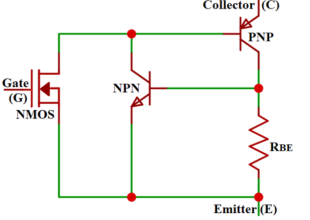
Figure 8. Internal structure
- IGBT has three terminals attached to three different metal layers, the metal layer of the gate terminal is insulated from the semiconductors by a layer of silicon dioxide (SIO2).
- IGBT is constructed with 4 layers of semiconductor sandwiched together. The layer closer to the collector is the p+ substrate layer above that is the n- layer, another p layer is kept closer to the emitter and inside the p layer, we have the n+ layers.
- The junction between the p+ layer and n- layer is called the junction J2 and the junction between the n- layer and the p layer is called the junction J1.
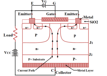
Figure 9. Construction of IGBT
Working:
- Consider a voltage source VG connected positively to the Gate terminal with respect to the Emitter. Consider other voltage source VCC connected across The Emitter and the Collector, where Collector is kept positive with respect to the Emitter.
- Due to the voltage source VCC the junction J1 will be forward-biased whereas the junction J2 will be reverse biased. Since J2 is in reverse bias there will not be any current flow inside the IGBT (from collector to emitter).
- Initially, when no voltage applied to the Gate terminal, at this stage the IGBT will be in non-conductive state. As we increase the applied gate voltage, due to the capacitance effect on the SiO2 layer the negative ions will get accumulated on the upper side of the layer and the positive ions will get accumulated on the lower side of the SiO2 layer.
- This will cause the insertion of negative charge carriers in the p region,
- The higher the applied voltage VG greater the insertion of negatively charged carriers. This will lead to a formation of the channel between the J2 junction which allows the flow of current from collector to emitter.
- The flow of current is represented as the current path in the picture, where the applied Gate voltage VG increases the amount of current flow therefore the collector to the emitter also increases.
Types of IGBT
IGBT is classified as two types based on the n+ buffer layer, the IGBTs that are having the n+ buffer layer is called the Punch through IGBT (PT-IGBT), the IGBTs that does not have an n+ buffer layer is called the Non-Punch Through- IGBT (NPT- IGBT).
Punch through IGBT (PT-IGBT) | Non-Punch Through- IGBT (NPT- IGBT) |
These are less rugged in short-circuit failure mode and has less thermal stability | These are more rugged in short circuit failure mode and has more thermal stability. |
The collector is a heavily doped P+layer | The collector is a lightly doped P+layer |
It has a small positive temperature coefficient of ON- State voltage, hence parallel operation requires great care and attention. | The temperature coefficient of ON-state voltage is strongly positive, hence the parallel operation is easy. |
The turn off loss is more temperature-sensitive, hence it increases significantly at a higher temperature. | The turn off a loss is less temperature-sensitive, so, it will remain unchanged with temperature.
|
IGBT Characteristics:
Static Characteristics
BVCES is the collector-emitter voltage at which no more than the specified collector current will flow at the specified temperature. This tracks the actual breakdown voltage.
As shown in Figure, BVCES has a positive temperature coefficient. At a fixed leakage current, an IGBT can block more voltage when hot than when cold.
For the example shown in Figure 8, at -50°C, BVCES is about 93% of the nominal 25°C specification.

Figure 10. Normalized Breakdown Voltage vs. Junction Temperature
RBVCES — Reverse Collector-Emitter Breakdown Voltage
This is the reverse collector-emitter breakdown voltage specification, i.e., when the emitter voltage is positive with respect to the collector. As with BVCES, RBVCES is the emitter-collector voltage at which no more than the specified emitter current will flow at the specified temperature.
VGE(th) — Gate Threshold Voltage
The gate-source voltage at which collector current begins to flow. Test conditions (collector current, collector-emitter voltage, junction temperature) are also specified. All
MOS gated devices exhibit variation in VGE (th) between devices, which is normal.
VCE(on) — Collector-Emitter on Voltage
This is the collector-emitter voltage across the IGBT at a specified collector current, gate-emitter voltage, and junction temperature. Since VCE(on) is temperature dependent, it is specified both at room temperature and hot.
As current increases, the temperature coefficient of a PT IGBT can actually transition from negative to positive.
ICES — Collector Cut-off Current
This is the leakage current that flows from collector to emitter when the device is off, at a specified collector emitter and gate-emitter voltage. Since leakage current increases with temperature, ICES is specified both at room temperature and hot. Leakage power loss is ICES times collector-emitter voltage.
IGES — gate-emitter leakage current
This is the leakage current that flows through the gate terminal at a specified gate-emitter voltage.
Dynamic characteristics
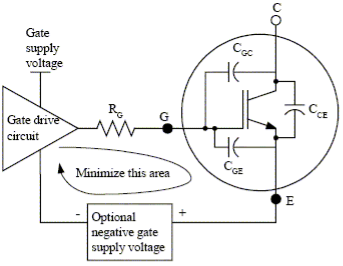
Figure 11. IGBT Capacitances Cies — Input Capacitance
This is the input capacitance measured between the gate and emitter terminals with the collector shorted to the emitter for AC signals. Cies is made up of the gate to collector capacitance (CGC) in parallel with the gate to emitter capacitance (CGE), or
Cies = CGE + CGC
The input capacitance must be charged to the threshold voltage before the device begins to turn on, and discharged to the plateau voltage before the device begins to turn off. Therefore, the impedance of the drive circuitry and Cies have a direct relationship to the turn on and turn off delays.
Coes — Output capacitance
This is the output capacitance measured between the collector and emitter terminals with the gate shorted to the emitter for AC voltages. Coes is made up of the collector to emitter capacitance (CCE) in parallel with the gate to collector capacitance (CGC), or
Coes = CCE + CGC
For soft switching applications, Coes is important because it can affect the resonance of the circuit.
Cres — Reverse transfer capacitance
This is the reverse transfer capacitance measured between the collector and gate terminals with the emitter connected to ground. The reverse transfer capacitance is equal to the gate to collector capacitance.
Cres = CGC

Figure 12 Capacitance vs. Collector-Emitter Voltage
VGEP — Plateau voltage
Figure 11 shows the gate-emitter voltage as a function of gate charge. The turn-on sequence traverses this curve from left to right, turn-off traverses from right to left. The gate plateau voltage VGEP is defined as the gate-emitter voltage when the slope of the gate-emitter voltage first reaches a minimum during the turn-on switching transition for a constant gate current drive condition

Figure 13 vGE as a Function of Gate Charge Qge,Qgc, and Qg — Gate Charge
Switching characteristics of IGBT:
The IGBT is a Voltage controlled device, hence it only requires a small voltage to the gate to stay in the conduction state. And since these are unidirectional devices, they can only switch current in the forward direction which is from collector to emitter.
A typical switching circuit of IGBT is shown below, the gate volt VG is applied to the gate pin to switch a motor (M) from a supply voltage V+. The resistor Rs is roughly used to limit the current through the motor.

Figure 14. Switching characteristics
The input characteristics of IGBT can be understood from the graph below.
Initially, when no voltage is applied to the gate pin the IGBT is in turn off condition and no current flows through the collector pin. When the voltage applied to the gate pin exceeds the threshold voltage, the IGBT starts conducting and the collector current IG starts to flow between the collector and emitter terminals. The collector current increases with respect to the gate voltage as shown in the graph below.


Figure 15. Output characteristics
- The output characteristics of IGBT have three stages,
- Initially, when the Gate Voltage VGE is zero the device is in the off state, this is called the cut-off region.
- When VGE is increased and if it is less than the threshold voltage then there will be a small leakage current flowing through the device, but the device will still be in the cut-off region.
- When the VGE is increased beyond the threshold voltage the device goes into the active region and the current starts flowing through the device. The flow of current will increase with an increase in the voltage VGE as shown in the graph above.
Key takeaways
- IGBTs are used in various applications such as AC and DC motor drives, Unregulated Power Supply (UPS), Switch Mode Power Supplies (SMPS.
- Traction motor control and induction heating, inverters, used to combine an isolated-gate FET for the control input and a bipolar power transistor as a switch in a single device, etc.
Static characteristics:
Drain-source on-state resistance (RDS(ON))
The resistance across drain and source when the MOSFET is in the "on" state.
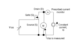
Figure 16. Static Characteristics
The specified constant drain current, ID, is applied until VGS reaches the specified voltage. At this point, drain-source voltage is measured. On-state resistance is calculated by dividing it by the value of drain current, ID.
Measurement of forward transfer admittance

Gate-source voltage, VGS, is increased until drain current, ID, reaches the specified value. Then, VGS is changed only slightly, and the resulting change in drain current, ID, is measured.
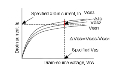
Figure 17 Change in VGS w.r.t ID
Dynamic Characteristics
Since power MOSFETs are majority-carrier devices, they are faster and capable of switching at higher frequencies than bipolar transistors.
Switching time measurement circuit and input / output waveform are shown below.
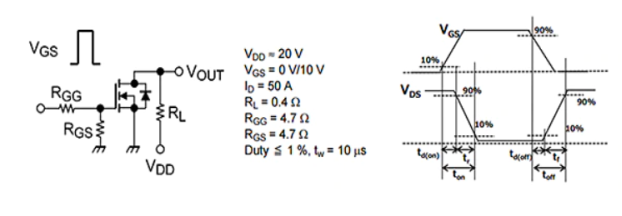
Figure 18. Dynamic Characteristics
td (on): Turn-on delay time
The time from when the gate-source voltage rises above 10% of VGS until the drain-source voltage reaches 90% of VDS
tr: Rise time
The time taken for the drain-source voltage to fall from 90% to 10% of VDS
ton: Turn-on time
The turn-on time is equal to td (on)+ tr.
td (off): Turn-off delay time
The time from when the gate-source voltage drops below 90% of VGS until the drain-source voltage reaches 10% of VDS
tf: Fall time
The time taken for the drain-source voltage to rise from 10% to 90% of VDS
toff: Turn-off time
The turn-off time is equal to td(off)+ tf.
Key takeaways
Features | MOSFET | IGBT |
Drive method | Voltage | Voltage |
Drive circuit | Simple |
|
Input Impedance | High | High |
Drive Power | Low | Low |
Switching Speed | Fast(ns) | Middle |
Operating Frequency | Fast (less than 1MHz) | Middle |
S.O. A | Wide | Wide |
Saturation | Voltage | High |
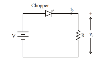
Principle of operation of chopper
Chopper circuits are known as DC to DC converters. Choppers are used to step up and step down the DC power. They change the fixed DC power to variable DC power. Using these, DC power supplied to the devices can be adjusted to the required amount.
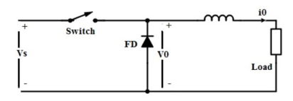
Figure 19. Chopper circuit
The principle of operation of chopper can be understood from the circuit diagram below.
The circuit consists of semiconductor diode, resistor, and load. For all type of chopper circuit, the output voltage value is controlled by periodic closing and opening of the switches used in the circuit.
The chopper can be viewed as an ON/OFF switch that can rapidly connect or disconnect the source to load connection. Continuous DC is given as source to the chopper as Vs and chopped DC is obtained across the load as V0.
Output Voltage and Current Waveforms
The output voltage and current waveforms of a chopper circuit are shown in figure. From the voltage waveform, it seen that during the period of TON the load voltage V0 is equal to the source voltage Vs.
But when the interval TOFF occurs, the DC voltage step downs to zero, thus making the load short-circuited.
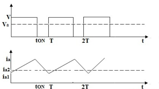
Figure 20. Output Waveform
- In the current waveform, during the interval TON the load current rises to the maximum value. During the interval TOFF, the load current decays.
- In TOFF condition the chopper is off so the load voltage becomes zero.
- But load current flows through the diode FD, making the load short-circuited.
- Thus, the chopped DC voltage is produced at the load.
- The current waveform is continuous which rises during TON state and decays during TOFF state.
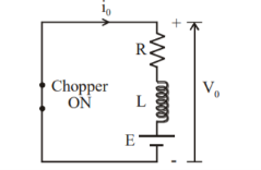
Class A Chopper
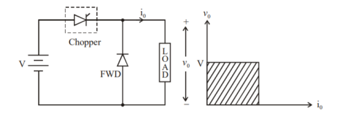
Figure 21 (a) Class A chopper
Figure shows a Class A Chopper circuit with inductive load and free-wheeling diode. When chopper is ON, supply voltage V is connected across the load that is current i0 flows as shown in figure.
When chopper is OFF, v0 = 0 and the load current continues to flow in the same direction through the free -wheeling diode. Therefore, the average values of output voltage and current are always positive. Hence, Class A Chopper is a first quadrant chopper (or single quadrant chopper).
Figure (b) shows output voltage and current waveforms for a continuous load current.

Figure 21 (b) Output voltage and current waveforms.
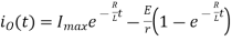
Class A Chopper is a step-down chopper in which power always flows from source to load. It is used to control the speed of dc motor. The output current equations obtained in step down chopper with R-L load can be used to study the performance of Class A Chopper.
CLASS B CHOPPER

Figure 22 Class B chopper
Fig. Shows a Class B Chopper circuit. When chopper is ON, and E drives a current through L and R in a direction opposite to that shown in figure. During the ON period of the chopper, the inductance L stores energy.
When Chopper is OFF, diode D conducts, and part of the energy stored in inductor L is returned to the supply. Also, the current continues to flow from the load to source. Hence the average output voltage is positive and average output current is negative.
Therefore, Class B Chopper operates in second quadrant. In this chopper, power flows from load to source. Class B Chopper is used for regenerative braking of dc motor.
Figure (b) shows the output voltage and current waveforms of a Class B Chopper. The output current equations can be obtained as follows. During the interval diode ‘D’ conducts (chopper is off) voltage equation is given by

For the initial condition i.e., at. The solution of the above equation is obtained along similar lines as in step-down chopper with R-L load
Therefore 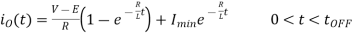
At 

During the interval chopper is ON voltage equation is given by

Redefining the time origin, at t=0, 
The solution for the stated initial condition is


Therefore 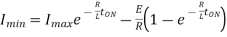
Figure 23. Class B Chopper Output Voltage and current waveform.
CLASS C CHOPPER
Class C Chopper is a combination of Class A and Class B Choppers. Figure a) shows a Class C two quadrant Chopper circuit.
For first quadrant operation, is ON or conducts and for second quadrant operation, is ON or conducts. When is ON, the load current is positive. i.e., flows in the direction as shown in figure
The output voltage is equal to V and the load receives power from the source.

Figure 24. Class C chopper
When CH1 is turned OFF, the energy stored in inductance L forces current to flow through the diode and the output voltage vo=0V, but io continues to flow in positive direction. When CH2 is triggered, the voltage E forces io to flow in opposite direction through L and CH2. The output voltage v0=0.
On turning OFF CH2 the energy stored in the inductance drives current through diode D1 and the supply.
The output voltage v0=V the input current becomes negative and power flows from load to source.
Thus, the average output voltage vo is positive but the average output current io can take both positive and negative values. Choppers CH1 and CH2 should not be turned ON simultaneously as it would result in short circuiting the supply.
Class C Chopper can be used both for dc motor control and regenerative braking of dc motor. Figure shows the output voltage and current waveforms.

Figure 25. Class C chopper output voltage and current waveform.
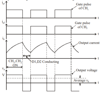
Class D chopper

Figure 26. D chopper
Figure shows a class D two quadrant chopper circuit. When both and are triggered simultaneously, the output voltage vo=V and output current Io flows through the load in the direction shown in figure.
When CH1 and CH2 are turned off the load io continues to flow in the same direction through load.
D1 and D2 due to energy stored in inductor L but output voltage vo = -V. The average load voltage vo is positive if chopper ON time (t ON) is more than OFF time t(OFF) and the average output voltage becomes negative if ton<toFF.
Hence, the direction of load current is always positive. But load voltage can be positive or negative.

Output voltage for ton>toff

Output voltage for ton<toff
Figure 27. Output waveforms.
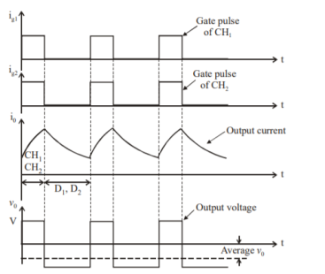
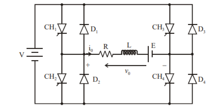
Class E chopper:

Four Quadrant Operation
Figure 28. Class E chopper
Figure shows a class E 4 quadrant chopper circuit. When they are triggered, output current flows in positive direction as shown in figure through and, with output voltage vo=V. This gives the first quadrant operation.
When both and are OFF, the energy stored in the inductor L drives through and in the same direction, but output voltage vo=-V. Therefore, the chopper operates in the fourth quadrant.
For fourth quadrant operation the direction of battery must be reversed. When Ch2 and Ch3 are triggered, the load current io flows in opposite direction and output voltage vo = -V. Since both io and vo are negative, the chopper operates in third quadrant.
When both CH2 and CH3 are OFF, the load current io continues to flow in the same direction through D1 and D4 and the output voltage vo=V. Therefore, the chopper operates in second quadrant as vo is positive but io is negative. Figure shows the devices which are operative in different quadrants.
Key takeaway
- Class A Chopper is a step-down chopper in which power always flows from source to load. It is used to control the speed of dc motor.
- Therefore, Class B Chopper operates in second quadrant. In this chopper, power flows from load to source. Class B Chopper is used for regenerative braking of dc motor.
- Class C Chopper can be used both for dc motor control and regenerative braking of dc motor. It is the combination of class A and class B chopper.
- Class D chopper can operate in different quadrants.
Solved Examples
Q1) A Chopper circuit is operating on TRC at a frequency of 2 kHz on a 460 V supply. If the load voltage is 350 volts, calculate the conduction period of the thyristor in each cycle.
A1)

Chopping period 

Output voltage 
Conduction period of thyristor


Q2) Input to the step up chopper is 200 V. The output required is 600 V. If the conducting time of thyristor is 200 µsec. Compute – Chopping frequency, – If the pulse width is halved for constant frequency of operation, find the new output voltage.
A2)


Solving for T
T=200s
Chopping frequency 
Pulse width is halved

Frequency is constant 
Output voltage 
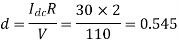
Q3) A dc chopper has a resistive load of 20Ω and input voltage VS = 220V. When chopper is ON, its voltage drop is 1.5 volts and chopping frequency is 10 kHz. If the duty cycle is 80%, determine the average output voltage and the chopper on time.
A3) 

 Voltage drops across chopper =1.5 volts
Average output voltage

 Voltage drops across chopper=1.5 volts
Average Output voltage

Chopper ON time 
Chopping period, 

Chopper ON time


Q4) In a dc chopper, the average load current is 30 Amps, chopping frequency is 250 Hz, supply voltage is 110 volts. Calculate the ON and OFF periods of the chopper if the load resistance is 2 ohms.
A4)


 and
and 


Chopper ON period

Chopper OFF period

CLC:( Current Limit control)
In DC to DC converter the current value varies between maximum and minimum level of constant voltage. In this method the DC to DC converter is turned On and Off to confirm that current is preserved constantly between upper limits and lower limits.
When the current energies beyond the extreme point Dc-Dc converter goes OFF.
When the switch is in its OFF state, current freewheels through the diode and falls in an exponential manner. The chopper is turned ON when the flow of current spreads the minimum level. This technique can be utilized either when the ON time ‘T’ is endless or when the frequency f=1/T.
Current Limit control
Figure 29. Current limit control
TRC (Time Ratio Control)
In time ratio control the value of the duty ratio, K =TON /T is changed. Here ‘K’ is called the duty cycle. There are two ways to achieve the time ration control, namely variable frequency, and constant frequency operation.
Constant Frequency Operation (PWM technique)
In constant frequency control strategy operation, the ON time TON is changed, keeping the frequency, that is f=1/T, or time period ‘T’ constant. This operation is also named as PWM (pulse width modulation control). Hence, the output voltage can be varied by varying ON time.
Figure 30 Constant Frequency Operation
Variable Frequency Operation (FM technique)
In variable frequency control strategy operation, the frequency (f = 1/T) is changed, then the time period ‘T’ is also changed. This is also named as a frequency modulation control. In both cases, the o/p voltage can be changed with the change in duty ratio.
Figure 31. Variable Frequency Operation
PWM Technique
The input dc voltage is of constant magnitude. The diode rectifier is used to rectify the line voltage. The inverter controls the magnitude and frequency of the ac output voltage. This is achieved by PWM technique of inverter switches and this is called PWM inverters. The sinusoidal PWM technique is one of the PWM technique to shape the output voltage to as close as sinusoidal output.
Basic concepts of switch mode inverter

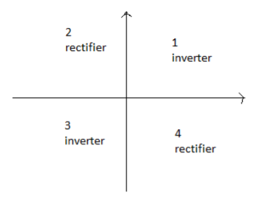
Figure 32 Operation as inverter and rectifier in different quadrants
During interval 1 𝑣0 and 𝑖0 both are positive
During interval 3 𝑣0 and 𝑖0 both are negative
Therefore during 1 and 3 the instantaneous power flow is from dc side to corresponding to inverter mode of operation. In contrast during interval 2 and 4 𝑣0 and 𝑖0 are of opposite sign i.e., power flows from ac side to dc side corresponding to rectifier mode of operation.
Pulse width modulated switching scheme
We require the inverter output to be sinusoidal with magnitude and frequency controllable. In order to produce sinusoidal output voltage at desired frequency a sinusoidal control signal at desired frequency is compared with a triangular waveform as show. The frequency of the triangular waveform established the inverter switching frequency. The triangular waveform is called carrier waveform. The triangular waveform establishes switching frequency 𝑓𝑠, which establishes with which the inverter switches are applied. The control signal has frequency 𝑓𝑠 and is used to modulate the switch duty ratio. 𝑓1 is the desired fundamental frequency of the output voltage.
The amplitude modulation ratio 𝑚𝑎 is defined as
ma = Vcontrol/Vtri
The frequency modulation ratio 𝑚f
mf = fs/f1
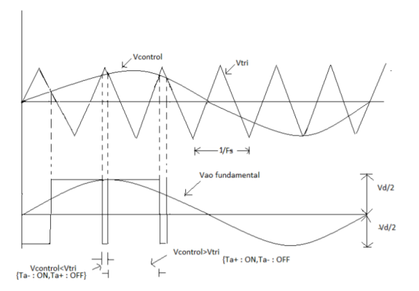
Figure 33 PWM Scheme
When 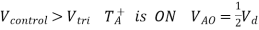
So, the following inferences can be drawn
The peak amplitude of fundamental frequency is  times
times 

Let the Vcontrol vary sinusoidal with frequency f1, which is the desired frequency of the inverter output voltage.
Let Vcontrol=V̂controlsin𝜔1t V̂control ≤ V̂tri

At 
So 


Key takeaway
In DC to DC converter the current value varies between maximum and minimum level of constant voltage. In this method the DC to DC converter is turned On and Off to confirm that current is preserved constantly between upper limits and lower limits.

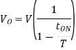
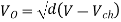
Figure 34. Step Up chopper
The figure shows Step Up chopper. To obtain load voltage Vo higher than the input voltage V. The values of L and C are chosen depending on the requirement of output voltage.
When the chopper is ON the inductor L is connected across the supply. The inductor current I rises and stores energy during ON time of the chopper tON.
When the chopper is off the inductor current is forced to flow through the diode D and load for a period t OFF. The current tends to decrease resulting in reversing the polarity of induced EMF in L. Therefore, voltage across load is given by
If a large capacitor ‘C’ is connected across the load, then the capacitor will provide a continuous output voltage. Diode D prevents any current flow from capacitor to the source. Step up choppers are used for regenerative braking of dc motors.
Expression for Output Voltage:
Assume the average inductor current to be I during ON and OFF time of Chopper.
When Chopper is ON
Voltage across inductor L=V
Therefore, energy stored in inductor = V.I.ton.
TOn = On period of chopper.
When Chopper is OFF (energy is supplied by inductor to load)
Voltage across L = V0 – V
Energy supplied by inductor L = (Vo-V) I t OFF
Where t OFF = OFF period of chopper.
Neglecting losses, energy stored in inductor L = energy supplied by inductor L
Therefore 
Where T=Chopping period or period of switching


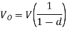
Where  duty cycle
For variation of duty cycle ‘d’ in the range 0<d<1 the output voltage Vo will vary in the range V<Vo<∞.
Problems:
A Chopper circuit is operating on TRC at a frequency of 2 kHz on a 460 V supply. If the load voltage is 350 volts, calculate the conduction period of the thyristor in each cycle.
V = 460 V Vdc = 350V, f=2KHz
Chopping period T = 1/f = 1/ 2 x 10 -3 = 0.5 m sec
Output voltage
Vdc = (tON/T) V
Conduction period of thyristor
TON = T x Vdc / V
TON = 0.5 x 10 -3 x 350 / 460 = 0.38 sec
Input to the step up chopper is 200 V. The output required is 600 V. If the conducting time of thyristor is 200 s sec. Compute Chopping frequency, If the pulse width is halved for constant frequency of operation, find the new output voltage.
Vs = 220V, R = 20 Ω, f = 10KHz.
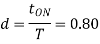
d = tON/T = 0.80
Vch = voltage drop across chopper = 1.5 Volts
Average output voltage
Vdc = (tON/T) (Vs-Vch) = 0.80(220-1.5) = 174.8Volts
Chopper ON time tON = dT
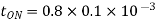
Chopping period T=1/f = 1/10 x 10 3 secs = 100 µsec
Chopper ON time
TON = dT
TOn = 0.80 x 0.1 x 10 -3 = 80 µ sec.
A dc chopper in figure has a resistive load of and input voltage of V = 200 V. When chopper is ON, its voltage drop is 2 V and the chopping frequency is 1 kHz. If the duty cycle is 60%, determine Average output voltage RMS value of output voltage Effective input resistance of chopper efficiency.

V=200V, R=10 , Chopper voltage drop,
  d=0.60, f=1 kHz
Average output voltage


RMS value of output voltage

Effective input resistance of chopper is

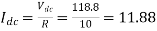 Amps
Amps
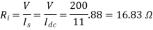
Output Power:


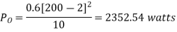
Input Power:


Chopper efficiency


Q) A chopper feeding on RL load is shown in figure, with V = 200 V, R = 5, L = 5 mH, f = 1 kHz, d = 0.5 and E = 0 V. Calculate – Maximum and minimum values of load current. – Average value of load current. – RMS load current. – Effective input resistance as seen by source. – RMS chopper current.
A)
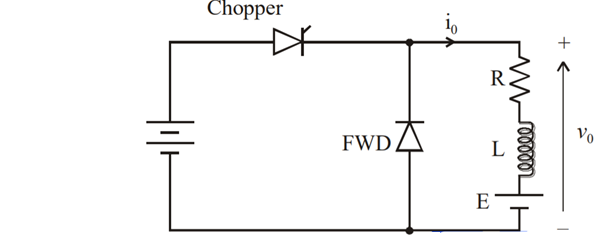
V=200V R=5
F=1kHz, d=0.5, E=0
Chopping period is
 secs
secs
Maximum value of load current is given by
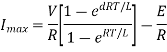
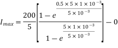

Minimum value of load current is given by


Average value of load current is

For linear variation of currents
RMS load current is given by


RMS chopper current is given by

Effective input resistance is

 Average source current
Therefore, effective input resistance is
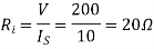
It is a type of DC to DC converter and it has a magnitude of output voltage.
The buck boost converter is equal to the flyback circuit and single inductor is used in the place of the transformer.
There are two types of converters in the buck boost converter that are buck converter and the other one is boost converter. These converters can produce the range of output voltage than the input voltage.
The following diagram shows the basic buck boost converter.

Figure 35 Buck Boost Converter
The working operation of the DC to DC converter is the inductor in the input resistance has the unexpected variation in the input current.
If the switch is ON, then the inductor feeds the energy from the input and it stores the energy of magnetic energy.
If the switch is closed it discharges the energy. The output circuit of the capacitor is assumed as high sufficient than the time constant of an RC circuit is high on the output stage.
The huge time constant is compared with the switching period and make sure that the steady state is a constant output voltage
Vo(t) = Vo(constant) and present at the load terminal.
There are two different types of working principles in the buck boost converter.
- Buck converter.
- Boost converter.
Buck Converter Working
The following diagram shows the working operation of the buck converter. In the buck converter first transistor is turned ON and second transistor is switched OFF due to high square wave frequency.
If the gate terminal of the first transistor is more than the current pass through the magnetic field, charging C, and it supplies the load. The D1 is the Schottky diode and it is turned OFF due to the positive voltage to the cathode.
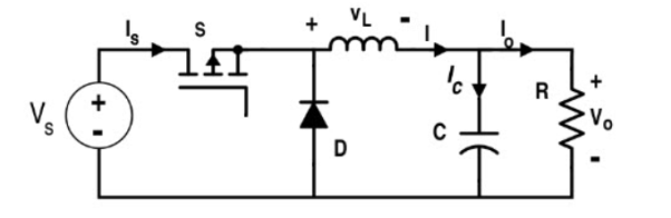
Figure 36. Buck Converter
The inductor L is the initial source of current. If the first transistor is OFF by using the control unit, then the current flow in the buck operation. The magnetic field of the inductor is collapsed and the back e.m.f is generated collapsing field turn around the polarity of the voltage across the inductor. The current flows in the diode D2, the load and the D1 diode will be turned ON.
The discharge of the inductor L decreases with the help of the current. During the first transistor is in one state the charge of the accumulator in the capacitor. The current flows through the load and during the off period keeping Vout reasonably. Hence it keeps the minimum ripple amplitude and Vout closes to the value of Vs
Boost Converter Working
In this converter the first transistor is switched ON continually and for the second transistor the square wave of high frequency is applied to the gate terminal.
The second transistor is in conducting when the on state and the input current flow from the inductor L through the second transistor.
The negative terminal charging up the magnetic field around the inductor. The D2 diode cannot conduct because the anode is on the potential ground by highly conducting the second transistor.
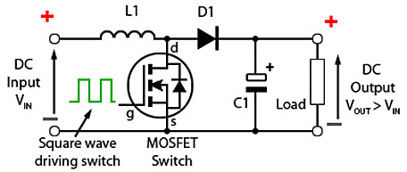
By charging the capacitor C the load is applied to the entire circuit in the ON State and it can construct earlier oscillator cycles. During the ON period the capacitor C can discharge regularly and the amount of high ripple frequency on the output voltage. The approximate potential difference is given by the equation below.
VS + VL
During the OFF period of second transistor the inductor L is charged and the capacitor C is discharged. The inductor L can produce the back e.m.f and the values are depending up on the rate of change of current of the second transistor switch. The amount of inductance the coil can occupy. Hence the back e.m.f can produce any different voltage through a wide range and determined by the design of the circuit. Hence the polarity of voltage across the inductor L has reversed now.
The input voltage gives the output voltage and atleast equal to or higher than the input voltage. The diode D2 is in forward biased and the current applied to the load current and it recharges the capacitors to VS + VL and it is ready for the second transistor.
Solved Examples
Q1) A transistor dc chopper circuit (Buck converter) is supplied with power form an ideal battery of 100 V. The load voltage waveform consists of rectangular pulses of duration 1 ms in an overall cycle time of 2.5 ms. Calculate, for resistive load of 10 Ω. (a) The duty cycle γ. (b) The average value of the output voltage Vo. (c) The rms value of the output voltage Vorms. (d) The ripple factor RF. (e) The output dc power.
A1)
(a) 
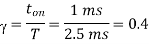
(b) 
(c)
(d) 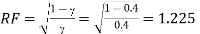
(e) 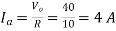

Q2) An 80 V battery supplies RL load through a DC chopper. The load has a freewheeling diode across it is composed of 0.4 H in series with 5Ω resistor. Load current, due to improper selection of frequency of chopping, varies widely between 9A and 10.2. (a) Find the average load voltage, current and the duty cycle of the chopper. (b) What is the operating frequency f? (c) Find the ripple current to maximum current ratio.
A2)
(a) The average load voltage and current are
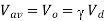

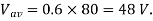
(b) to find the operating (chopping) frequency
During the ON period

Assume  constant

From eq (1)


But 
Hence 
The maximum current  occurs at =1
Ripple current 

Q3) A DC Buck converter operates at frequency of 1 kHz from 100V DC source supplying a 10 Ω resistive load. The inductive component of the load is 50mH.For output average voltage of 50V volts, find: (a) The duty cycle (b) ton (c) The rms value of the output current (d) The average value of the output current (e) Imax and Imin (f) The input power (g) The peak-to-peak ripple current.
A3)
(a) 

(b) 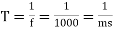


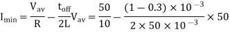

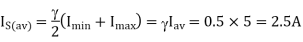

(g) 
Batteries are the primary energy-storage devices in ground vehicles. Now days battery fed electric drives are commonly being used for electric vehicles applications, due to various advantages, such as: nearly zero emission, guaranteed load leveling, good transient operation and energy recovery during braking operation. To fulfil these requirements converters with bidirectional power flow capabilities are required to connect the accumulator (battery) to the dc link of the motor drive system.
Battery fed electric vehicles (BFEVs) is required to function in three different modes namely: acceleration mode, normal (steady-state) mode and braking (regenerative) mode. During acceleration and normal modes, the power flow is from battery to motor whereas during braking or regenerative mode the kinetic energy of the motor is converted into electrical energy and fed back to battery.
The DC-DC converter is required to perform mainly two functions: first to match the battery voltage to the motor rated voltage and second to control the power flow under steady-state and transient conditions, so that the drive performance is as per the requirement.
The use of a Bi-directional dc-dc converter for a battery fed electric vehicle drive system. A closed loop speed control technique of the proposed battery fed electric vehicle is designed and implemented using PI controller. The overall drive system reduces the system complexity, cost and size of a purely electric based vehicular system.

Figure 37 Circuit Diagram
Above figure shows the proposed Bi-directional dc-dc converter fed DC motor drive. In this topology, boost converter operation is achieved by modulating Q2 with the anti-parallel diode D1 serving as the boost mode diode. With the direction of power flow reversed, the topology functions as a buck converter through the modulation of Q1, with the anti-parallel diode D2 serving as the buck-mode diode. It should be noted that the two modes have opposite inductor current directions.
A new control model is developed using PI controller to achieve both motoring and regenerative braking of the motor. A Lithium-ion battery model has been used in this model to verify the motor performance in both motoring and regenerative mode. This controller shows satisfactory result in different driving speed commands.
For the dc–dc converter, the only important part of the inverter–machine subsystem is the zero-sequence impedance and the zero-sequence voltage vz. Thus, the integrated dc–dc converter can be modeled. The time-dependent voltage source vz represents the zero-sequence voltage and vs4 describes the voltage across ss4. These two voltage sources are connected to an LR circuit, modeling the machine’s zero-sequence impedance. Voltage vt represents the transformer voltage.
It has to be mentioned that vz, can only be measured if no zero-sequence current flows; otherwise, it is a theoretical quantity since there is a voltage drop vlr across L0 and R0. The voltage measured between the star point and the negative bus is equal to vz −vlr. This system is similar to a full-bridge rectifier system, but as the voltage vz applied to the system is neither average free (related to the switching frequency) nor free from even harmonics, a conventional modulation scheme cannot be adopted.
In the actual implementation, an active rectifier is used to guarantee that the voltage-time product across the transformer remains below a predetermined level. The described dc– dc con- verter is similar to a dual active bridge. A unidirectional implementation with a diode rectifier would be an-Converter waveforms: zero-sequence voltage vz, voltage vs4 across s4, voltage vt1 across st1, voltage vt2 across st2, and transformer voltage vt. Other possibility, but in order to limit the voltage-time product across the transformer, a special control approach has to be implemented.
Equations
The bi-directional converter is designed based on the input supply voltage and output voltage requirement to drive the electric vehicle at desired speed. The converter power topology is based on a half bridge circuit to control the dc motor. At a given input battery voltage and reference speed command the inductor current has a nearly constant peak to peak swing. The inductor is designed with a specified current ripple of 15A and 20 KHz switching frequency.
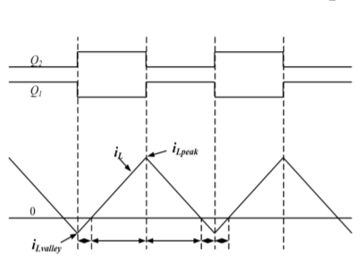
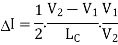

References:
- Vedam Subramanyam - Power Electronics, New Age International, New Delhi.
- Dubey, Donalda, Joshi, Sinha, Thyristorised Power controllers, Wiley Eastern New Delhi.
- M. D. Singh and K. B. Khandchandani, Power Electronics, Tata McGraw Hill.
- Jai P. Agrawal, Power Electronics systems theory and design LPE, Pearson Education, Asia.
- L. Umanand, Power Electronics – Essentials and Applications Wiley Publication.
- J. Michael Jacob – Power Electronics Principal and Applications.
- M. H. Rashid - Power Electronics Handbook, Butterworth-Heinemann publication, 3rd edition.
- S. Williamson, M. Lukic, and A. Emadi, “Comprehensive drive train efficiencyanalysisofhybridelectricandfuel cell vehicles based on motor- controller efficiency modeling,” IEEE Trans. Power Electron., vol. 21, no. 3, pp. 730–740, May 2006.
- A. Emadi, S. Williamson, and A. Khaligh, “Power electronics intensive solutions for advanced electric, hybrid electric, and fuel cell vehicular power systems,” IEEE Trans. Power Electron., vol. 21, no. 3, pp. 567– 577, May 2006.
- A. Emadi, M. Ehsani, and J. Miller, “Advanced silicon rich automotive electrical power systems,” in Proc. 18th Digit. Avionics Syst. Conf., St Louis, MO, Oct. 24–29, 1999, vol. 2, pp. 8.B.1-1–8.B.1-8.


