Unit-6
Network Functions
Discussed in detail in section 6.3
A) One port Network:-
The one-port network can be represented as shown below. it has only one port i.e. input port or only output port.
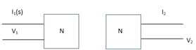
fig 1) one-port networks
1) Driving point impedance at the input port
Z11(S) = V1(S) / I1(S)
2) Driving point impedance at the output port
Z22(S) = V2(S) / I2(S)
3) Driving point admittance at the input port
Y11(S) = I2(S) / V2(S)
4) Driving point admittance at the output port
Y22(S) = I2(S) / V2(S)
After studying the above equations, it can be that
Z11(S) = 1 / Y11(S) And Z22(S)=1/Y22(S)
B) Two Port Network:-
The network as the name says has two one input and the other output port.
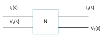
Fig 2) Two-port network
1)Transfer Function impedance Z11(S) = V2(S) / I1(S)
2) Transfer admittance function Y12(S) = I2(S) / V1(S)
3) Current ratio transfer function Y12(S) = I2(S) / I1(S)
4)Voltage ration transfer function G12(S) / V2(S) / V1(S)
Key takeaway
Z11(S) = V1(S) / I1(S)
Z11(S) = V2(S) / I1(S)
Q1) For the network shown below 1)show that with port 2)open the driving point input impedance 1π)b)find the voltage, ratio transfer function 1/2 for the two-port network.
Solution: From the above network we take L.T
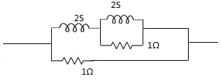
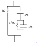
Fig 3 Laplace Transform for the above circuit
Reducing 4 we gel,
Z1=(25+25*1 / 25+1)*1
25+25*1 / 25+1*1
Z1=4S2+45/452+65+1
Z2=
Z2=(1/4S/1/4+1/5+1/5)*2
1/45/1/4+1/3+1/5+2
=2(5+5+4) / 5+5+4+25(5+4) = 2(25+4)/252+10S+4
Z2=25+4/252+10+4
Applying KVL, in the circuit
V1=I1Z1+I,Z2 -----------1
V2= I1Z2 ...............2
.: V1=I1Z1+V
V1 / I1= (Z1+Z2) (from----1)
Dividing equation 2 by 1
G12=Z 2 / Z1+Z2
calculating z11 we have,
Z11=Z1+Z2
Z11 = 4S2+4S / 4S2+6S+1 * 2S+4/S2+SS+2
=(4S2+4S)(S2+SS+2)+(2S+4)(4S2+6S+1) / (4S2+6S+1)(S2+SS+2)
Z11=4S4+20S3+8S2+4S3+20S2+8S+8S3+12S2+25+16S2+4 /(4S2+6S+1)(S2+SS+2)
= (4S4+32S3+5652+345+4 / (4S2+6S+1)(S2+SS+2)
G12= Z2 / Z1+Z2
= (2S+4) / (S2+SS+2) / (4S+32S3+56S2+34S+4) / (4S2+6S+1)(S2+SS+)
G12= (2S+4)(4S2+6S+1) / 4S4+32S3+56S2+34S+4
Network function of some network and general network
a) Ladder Network:-
For this type of network, series are represented as impedance, and Shunt have represented admittance, as shown below
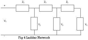
now we can find the transfer function of the above network KCL and KVL and then substituting the value in each equation the equation is reached which relative the output to input.
Z=Z1+ 1 /Y2+1/
Z3+ 1/
Y4+1/Z5+1/Y6
Hare, first Y6 is converted as Z6(=1 / Y6) Then combined with Z5 and this is called continued function method.
b) Non-Ladder Network:-
The bias non-ladder networks are below where the value of transfer in penance and admittance is obtained as
a)Bridged-T network
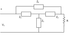
Fig 5 Bridged T Network
b) Twin-t network
Fig 6 Twin-T Network
c) Lattice network
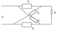
Fig 7 Lattice Network
Where,
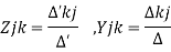
∆- nodded basis determinant
∆- Loop basis determinant
∆’kj , ∆ jk- cofactor
voltage ration transfer function 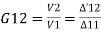
Current raw transfer function 
Key takeaway
For lattice network, the series elements are represented as impedance and Shunt are represent admittance
Let us consider the following transfer function
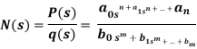
a, b- coefficient with are real and positive
Features of poles and zeros of network function.
a) The network function is described by poles and zeros.
b) The zeros of the network exit for the complex frequencies where N(s)=0
c) The poles of the network exits for the complex frequencies where N(s)=o
d)The number of poles is equal to some zeros considering types poles and zeros which at infinity.
e)when n>m, poles at infinity has a degree(n-m)
f)When m>n, zeros at infinity with a degree (m-n)
g) The time variation response of the network is determined through the poles.
h) The magnitude of response is determined by poles and zeros of the network function.
i) If q(s) =0, is the characteristics equation of N(S).
J) Capacitor is represented as (ʊ)=1/cs so, for
S = 0, It behaves like open circuits
S= behaves as a short circuit
k)for inductor z(s) = Ls so, for
s= o It behaves short circuit
s = It behaves as given circuits
Key takeaway
The zeros of the network exit for the complex frequencies where N(s)=0
The poles of the network exist for the complex frequencies where N(s)=o
Que) For the network shown, find driving point input impedance .plot the pole-zero patterns for each as well.
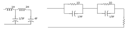
Fig 8 (1) Circuit Diagram Fig 8(2) Circuit Diagram
Solution - For Fig 8(1) taking L.T we have
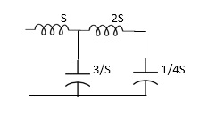
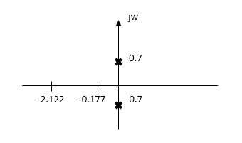
Fig 9 Laplace for Fig 8(1) with roots
Z11= 1+ 1 /S/3+1/25+1/1/4S
=1+ 1/ 5/3+1/6S
=1+ 18S/6S2+3
Z11=6S2+3+18S/ 6S2+3 =2S2+6S+2/2S2+1
Zeros of equations are taking lt.of circuit b)
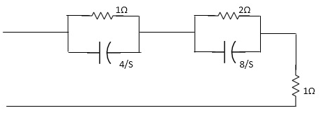
Fig 10 Laplace for Fig 8(2)
Z11= 1*4/5
1+4/5+2.8/3/2+8/5+1
=4/5+4 + 16/ 25+8+1
= 4/5+4+8/5+4+1
=s+12+4/(5+4)
Z11= S+16/(S+4)
For zeros of system
s+16=0
s=-16
for poles of system
s+4=0
s=-4
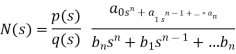
N(s) =p(s) =qosn+q,sn--------an/ q(s) bosn+b,sn-----------bn
1) All coefficient of p(s) and q(s) should be real and positive
2) poles and zeros must be conjugate whether imaginary or complex
3) Real part of poles and zeros must be negative or zero.
4) The degree of p(s) may differ either by zero or 1.
5) Lowest degree of p(s) and q(s) may differ at the most by one.
6) p(s) and q(s) cannot have missing terms between highest and lowest degree unless all when or all odd terms are missing.
Q) Find whether the following network function represents the driving point function.
a) f(s)= (s+1)/(s2+1) b) f(s) = 3s2+2s+1/ss3+9s2+3s+2 c) f(s)=(s2+1)2/s2(s+3)
solution
a) f(s)=s+1/s2+1
It represents the driving point function:
b) F(S)= 3S2+2S+1 / 5S3+9S2+3S+2
It represents the driving point function.
b)F(s)=3s2+2s+1/5s3+9s2+3s+2
It represents the driving point function
c) f(s) = (s2+1)2/s2(5+3)
It has representative zeros, hence not valid
( s2+1)2=0
s2=+-1
s2=+-j,+-j
v) Restriction as transfer function-
a) All coefficients of p(s) and q(s) should be real and positive for q(s)
b) The poles must be conjugate if imaginary or complex.
c) The real part of poles must be negative or new of zero than pole must be simple.
d)The degree of p(s) could be zero and it is independent of q(s) for example f(s) 5/ (s3+3s+1)
e) q(s) cannot have missing terms between the highest and lowest degree unless all the even or all odd terms are missing
f) degree of q(s) >,p(s)
g) p(s) may have missing terms between the highest and lowest degree and its coefficients could be negative.
Key takeaway
The degree of q(s) >p(s).
All coefficients of p(s) and q(s) should be real and positive for q(s)
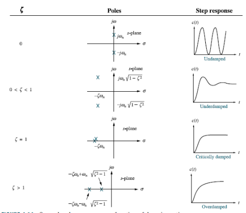
To find the time domain behaviour we consider a simple RLC circuit. when the poles and zeros of I(s) can be represented in terms of undammed nautical frequency (wn)and damping ratio  . these can be represented as.
Wn = 1/ Lc and
  =R/2
=R/2 C/L
C/L
For RLC network the characteristics equation of any second differential equation.
s2+2 wns+wn2=0
s1s2=-2 wn+-
wn+-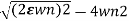 / 2
/ 2
=-2 wn+-
wn+- /2
/2
=-2 wn+-
wn+- /2
/2
=-2 wn+-2
wn+-2 / 2
/ 2
s1,s2 =- wn+-wn
so, depending an § poles can be represented in various ways
a)  >1
>1
s1s2 = - wn+- wn
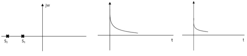
Fig 11 Location of Poles and system response
As s1 s2 lies on the negative real axis. This corresponds to OVERDAMPED are has exponential decay from in the time domain.
b) 0< <1
<1
s1s2 = - wn+-∫wn
The poles are plotted below having both real and the imaging part
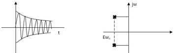
Fig 12 Time response Fig 13 Root Plot
As the poles have real and imaginary components as roots 0, this corresponds to the UNDERDAMPED association. As initially, oscillations exist, but oscillations are seen as t-
c)  =0
=0
s1s2 = - wn+- wn
s2+2 wns+w2n=0
for  =0
=0
s2+wn2=0
s=Ijwn
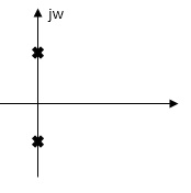
Fig 14 Root Plot Fig 15 Time response
As the complex conjugal the as at t=0 and t= same so, this is the case of UNDAMPED associations.
Key takeaway
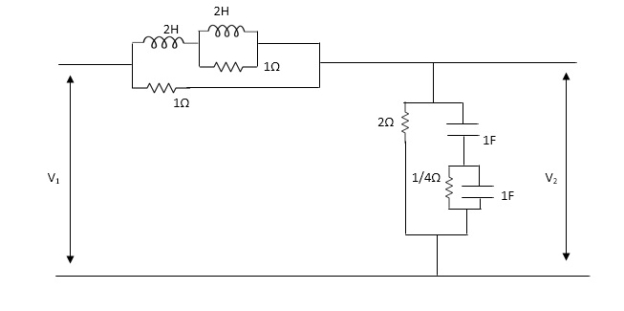
Q. For network below 1), the pole-zero pattern is represented in fig 16), find the numerical value of R, L, and c for z (0) =1?
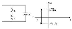
Fig 16 Pole zero plot
Solution
Calculating z(s) by taking L.T of fig 1)
z(s) = (R+SL)*1/CS
(R+SL)+1/CS = R+SL / SRC+S2LC+1
Z(S)= S+R/L / C [S2+R/L S+1/LC]
Given z(0)=1
z(0)=R/L / C/LC =1
Z(0)=R=1
.: R=1
Polls are given as
S2+RS/L+1/LC=0
S=-R/2L +J
Zeros are given as
S+R / L=0
From pole zero plot value of pole location is at -1 so
-R / L = -1
-1/ L=-1
L=1H
Also imaginary part of pole from plot is
 =
=
1/LC-(R/2L)2 =11/4
1/C-(1/2)2=11/4
1/C-1/4=11/4
1/C=11/4+1/4
1/C=12/4 =3
C=1/3 F
Hence, the value of R=1 L=14 and c=1/3 f
Q . FOR the following circuits, FIND G12(S) =v2/v1
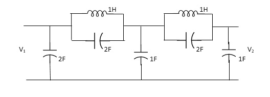
Solution Taking Laplace transform of above we have
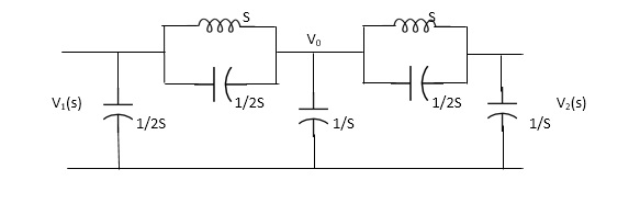
Fig 17 Laplace Transform of the above circuit
Applying KCL at node v0
V0-V1(S) / S*1/2S/(S+1/2S) +V0+V2(S)/ (S*1/2S)/(S+1/2S)+V0/1/S=0
For Porr 2)We have ,
v2-v0/(s*1/2s)/(s+1/2s)+v2/1/s =0 ---------(ii)
(v2-v0)(2s2+1) / s +sv2=0
v2 [2s2+1/s+s] = v0( 2s2+1)/ s
v0=v2(3s2+1) / (2s2+1)-----------(iii)
from (i) we have ,
(v0-v1) /s (2s2+1) *sv0+(v0-v2)/5 (s2+1) =0
(2s2+1/5)v0-(2s2+1)/sv1+sv0+(2s2+1)/sv0-(s2+1)/s v2=0
(2s2+1)v1=(5s2+2)v0-(2s2+1)v2
substitute value v0 from (iii) above
(2s2+1)v1 =[( 5s2+2)(3s2+1) /(2s2+1)-(2s2+1)]v2
(2s2+1)v1=(15s4+5s2+6s2+2-4s4+4s2) / (2s2+1 *v2
G12(s) = v2/v1 = (2s2+1) 2/11s4+15s2+1
Q) Find the transfer function admittance ratio
Y12(s) = I2(S) / V1(S)
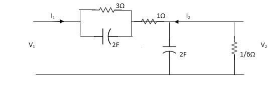
Solution = Taking Laplace transform of the above figure
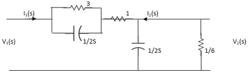
Fig 18 Laplace Transform of the above circuit
Applying KCL we get,
(V2-V1) / (3*1/2S) / (3+1/2S) * V2/ 1/2S+ V2/1/6 =0
(Y2-V1)(6S+1) / (6S+4) * (2S+6)V2V=0
BUT I2=-6V2
V2=-I2/6
We have ,
(6s+1) / (6s+4)*v2-(6s+1) / (6s+4)*v1 +(2s+6)v2=0
-[6s+1 / 6s+s+2s+6]I2 / 6 =V1(6S+1) / 6S+4
-[6S+1(2S+6)(6S+4)]I2= 6(6S+1)V1
-[(6S+1)*12S2+36S+8S+24] I2=6(6S+1)
I2 / V1 =-6(6S+1) / 12S2+50S+25
Y12(S) = I2(S) / V1(S) = -6(6S+1) / 12S2+50S+25
The elements which deliver power or energy is called active elements, used for amplification purpose.
For eg: transistor, voltage, and current source
Power Delivered and Power Absorbed :
Passive elements (R, L, or C) absorbs power.
Power delivered –ve
Power absorbed +ve
If current enters at positive polarity then the element absorbs power.
If the current leaves at a positive terminal then the element delivers power.
Q – Find whether the sources absorb or delivers power?
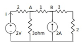
Sol : Apply kcl at A
Va – 2 / 2 + Va / 3 + Va – Vb / 1 = 0
11Va – 6Vb = 6 ---(1)
Apply kcl at B
VB – VA / 1 + VB / 5 – 2 = 0
-5VA + 6VB = 10 ---(2)
From (1) & (2)
VA = 8/3V, VB = 35/9V
i = 2 – Va / 2 = -1/3A
Since, current leaves positive Terminal so, the element delivers power.
= -[ 2 x (-1/3) ] = -2/3
Or
Power absorb = 2/3 watts ( For voltage source )
For current source power delivered
= 35/9 x (-1/3)
= -70/9 watts
Power delivered + Power absorbed = 0
-70/9 + 2/3 + power absorbed by ‘ R ’ = 0
Power absorbed by resistance = 64 / 9 watts
Necessary Conditions for Stable Driving Point Functions:
After canceling the common factors in the numerator polynomial P(s) and denominator polynomial Q(s), the necessary conditions for the driving point functions are as follows :

Key takeaway
The elements which deliver power or energy is called active elements, used for amplification purpose.
If current enters at positive polarity then the element absorbs power.
If the current leaves at a positive terminal then the element delivers power.
Definition: it is defined as the phenomenon which takes place in the series or parallels the R-L-C circuit which leads to a unity power factor
Voltage and current in R – L - C ckt. Are in phase with each other
Resonance is used in many communication circuits such as a radio receiver.
Resonance in series RLC series resonance in parallel RLC anti-resonance / parallel resonance.
Xc =  - capacitive reactance
At a particular frequency ȴ = fr, the Inductive and capacitive reactance are exactly equal
 XL = XC ……at ȴ = fr
Ie  L =
L = 
 fr2 =
fr2 = 
 fr =
fr =  H2
H2
And  = wr =
  rad/sec
Quality factor / Q factor
The quality of resonance circuit is measured in terms of efficiency of L and C to stare energy and the efficiency of L and C to store energy as measured in terms of a factor called quality factor or Q factor it is expressed as
Q =  and Q =
The sharpness of tuning of the R-L-C series circuit or its selectivity is measured by the value of Q. as the value of Q increases, the sharpness of the curve also increases, and the selectivity increases.
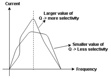
Fig 19 Response of RLC parallel circuit
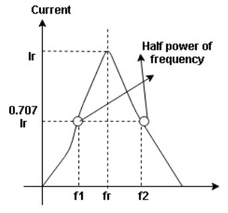
Fig 20 Bandwidth of Resonant Circuit
Bandwidth (BW) = f2 = b1
 and
and  are the frequency at which the power delivered to the resistor is reduced to 50% of the power delivered to it at resonance
  these frequencies are called half-power frequency
Bw = fr/Q
Resonance in Parallel circuit:
When a coil is in parallel with a capacitor, as shown below. The circuit is said to be in resonance.
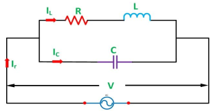
Fig 21 Parallel Resonant Circuit
The resonant frequency for the above circuit is fr =  Hz
Hz
The current at resonance is I=
The value L/RC is known as dynamic impedance.
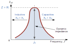
Fig 22 Characteristics of RLC parallel circuit
The current at resonance is minimum. The circuit's admittance must be at its minimum and one of the characteristics of a parallel resonance circuit is that admittance is very low limiting the circuit's current. Unlike the series resonance circuit, the resistor in a parallel resonance circuit has a damping effect on the circuit bandwidth making the circuit less selective.
Also, since the circuit current is constant for any value of impedance, Z, the voltage across a parallel resonance circuit will have the same shape as the total impedance and for a parallel circuit, the voltage waveform is generally taken from across the capacitor.
Bandwidth and selectivity:
 and
and  are the frequency at which the power delivered to the resistor is reduced to 50% of the power delivered to it at resonance
  these frequencies are called half-power frequency
Bw = fr/Q
Q =  =
=  fCR = R
Resonant Frequency:
The resonant frequency for the parallel resonant circuit is given as
fR= 
Where L= inductance of the coil
C = is the capacitance
Rs = Resistive value of coil.
Key takeaway
The resonant frequency for the parallel resonant circuit is given as
fR= 
Bw = fr/Q
Q =  =
=  fCR = R
Condition for resonance XL = XC
Que) A coil takes a current of 6A when connected to a 24V dc supply. To obtain the same current with 50HZ ac, the voltage required was 30V. Calculate inductance and p.f of the coil?
Sol: The coil will offer only resistance to dc voltage and impedance to ac voltage
R =24/6 = 4ohm
Z= 30/6 = 5ohm
XL = 
= 3ohm
cosφ =  = 4/5 = 0.8 lagging
Que) The potential difference measured across a coil is 4.5V when it carries a DC of 8A. The same coil when carries AC of 8A at 25Hz, the potential difference is 24V. Find current and power when supplied by 50V,50Hz supply?
Sol: R=V/I= 4.5/8 = 0.56ohm
At 25Hz, Z= V/I=24/8 =3ohms
XL = 
= 2.93ohm
XL = 2 fL = 2
 x 25x L = 2.93
L=0.0187ohm
At 50Hz
XL = 2x3 =6ohm
Z =  = 5.97ohm
I= 50/5.97 = 8.37A
Power = I2R = 39.28W
Que) A coil having an inductance of 50mH and resistance 10ohmis connected in series with a 25 F capacitor across a 200V ac supply. Calculate resonant frequency and the current flowing at resonance?
Sol: f0= = 142.3Hz
I0 = V/R = 200/10 = 20A
Que) A 15mH inductor is in series with a parallel combination of an 80ohm resistor and 20 F capacitors. If the angular frequency of the applied voltage is 1000rad/s find admittance?
Sol: XL = 2 fL = 1000x15x10-3 = 15ohm
XL = 1/ C = 50ohm
Impedance of parallel combination Z = 80||-j50 = 22.5-j36
Total impedance = j15+22.5-j36 = 22.5-j21
Admittance Y= 1/Z = 0.023-j0.022 siemens
Que) A circuit connected to a 100V, 50 Hz supply takes 0.8A at a p.f of 0.3 lagging. Calculate the resistance and inductance of the circuit when connected in series and parallel?
Sol: For series Z =100/0.8 = 125ohm
cosφ = 
R = 0.3 x 125 = 37.5ohm
XL =  = 119.2ohm
XL = 2 fL = 2
 x 50x L
119.2 = 2 x 50x L
L= 0.38H
For parallel:
Active component of current = 0.8 cosφ = 0.3x0.3 = 0.24A
R = 100/0.24 =416.7ohm
Quadrature component of current = 0.8 sinφ = 0.763
XL= 100/0.763 = 131.06ohm
L= 100/0.763x2 x50 = 0.417H
Reference
[1] Network Analysis Third Edition by M. E. Van Valkenburg, Prentice Hall of India Private Limited.
[2] Network Analysis & Synthesis by G. K. Mittal, Khanna Publication.
[3] Network Analysis and Synthesis by Ravish R Singh, McGraw Hill.
[4] Introduction to Electric Circuits by Alexander & Sadiku, McGraw Hill.
[5] Introduction to Electric Circuits by S. Charkarboorty, Dhanpat Rai & Co.
[6] Fundamentals of Electrical Networks by B.R.Gupta & Vandana Singhal- S.Chand Publications
[7] Electrical Circuit Analysis 2nd Edition by P. Ramesh babu, Scitech Publication
India Pvt Ltd.


