Unit - 4
IIR Filter Design & Realization
Filters are networks that process signals in a frequency-dependent manner. The basic concept of a filter can be explained by examining the frequency dependent nature of the impedance of capacitors and inductors. Consider a voltage divider where the shunt leg is a reactive impedance.
As the frequency is changed, the value of the reactive impedance changes, and the voltage divider ratio changes. This mechanism yields the frequency dependent change in the input/output transfer function that is defined as the frequency response.
A simple, single-pole, high-pass filter can be used to block dc offset in high gain amplifiers or single supply circuits. Filters can be used to separate signals, passing those of interest, and attenuating the unwanted frequencies.


Fig: Basic Analog Filters
Key takeaway
Sr. No | Analog filter | Digital filter |
1. | Analog filters are used for filtering analog signals. | Digital filters are used for filtering digital sequences |
2. | Analog filters are designed with various components like resistor, inductor and capacitor. | Digital filters are designed with digital hardware like FF, counters shift registers, ALU and software’s like C or assemble language. |
3 | Analog filters less accurate and because of component tolerance of active components and more sensitive to environmental changes | Digital filters are less sensitive to the environmental changes, noise and disturbances. Thus periodic calibration can be avoided. Also they are extremely stable. |
4. | Less flexible | These are most flexible as software programs & control programs can be easily modified. Several input signals can be filtered by one digital filter. |
5. | Filter representation is in terms of system components | Digital filters are represented by the difference equation. |
6 | An analog filter can only be change by redesigning the filter circuit. | A digital is programmable ie its operation is determined by a program stored in the processor’s memory. This means the digital filter can easily be changed without affecting the circuitry (hardware). |
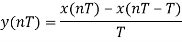
Consider an analog filter. It’s transfer function will be of the differential equation form as shown below.

Taking Laplace transform on both ends:

The transfer function of the analog filter can be given by:

Note that this is just a generic transfer function. To get the transfer function of a digital filter we will dive into some specifics.
Thus,

Taking z-transform on both sides:
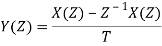
Solving for the transfer function of the digital filter:
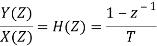
The mapping between S and Z planes
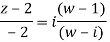
To map from s to z-plane we need to find the values of σ and Ω in s = σ + jΩ. We have the relationship between s and z from above as:

Rewriting the above equation for z:

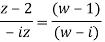
Substituting s = σ+jΩ in the above equation and solving gives us:

Separating the real and imaginary parts we get:
For σ=0

When we vary Ω from -∞ to +∞, the corresponding locus of points in the z-plane is a circle with radius 1/2 and with its center at z=1/2.
Similarly, when we map the equation  the left half-plane of the s-domain maps inside the circle with 0.5 radians. Moreover, the right half-plane of the s-domain is mapped outside the unit circle.
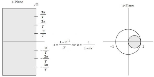
Fig: Mapping of S and z-plane
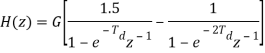
Mapping of s-plane into the z-plane by the approximation of derivatives method.
Thus, we can say that this transformation of an analog filter results in a stable digital filter.
Limitations:
From the above fig, the location of poles in the z-domain is confined to smaller frequencies. Thus the approximation of derivatives method is limited to designing low pass and bandpass IIR filters with small resonant frequencies only. It can’t be used to develop high pass and band-reject filters.
Key takeaway
From the above fig, the location of poles in the z-domain is confined to smaller frequencies. Thus, the approximation of derivatives method is limited to designing low pass and bandpass IIR filters with small resonant frequencies only. It can’t be used to develop high pass and band-reject filters.
Numerical:
Q. Design a Discrete Time Low Pass Filter for a voice signal. The specifications are: Passband Fp 4 kHz, with 0.8 dB ripple; Stopband FS 4.5 kHz, with 50dB attenuation; Sampling Frequency Fs 22 kHz. Determine a) the discrete time Passband and Stopband frequencies, b) the maximum and minimum values of H () in the Passband and the Stopband, where () is the filter frequency response.
Solution
a) Recall the mapping from analog to digital frequency 2 F/Fs , with Fs the sampling frequency. Then the passband and stopband frequencies become p 2 4/ 22 rad 0.36 rad, s 2 4.5/ 22 rad 0.41 rad;
b) A 0.8 dB ripple means that the frequency response in the passband is within the interval 1 where is such that 20 log10 (1+) 0.8 This yields 100.04 1 0.096.
Therefore the frequency response within the passband is within the interval 0.9035 H() 1.096. Similarly in the stopband the maximum value is () 1050/20 0.0031
The Impulse Invariance Method is used to design a discrete filter that yields a similar frequency response to that of an analog filter. Discrete filters are amazing for two very significant reasons:
- You can separate signals that have been fused and,
- You can use them to retrieve signals that have been distorted.
We can design this filter by finding out one very important piece of information i.e., the impulse response of the analog filter. By sampling the response we will get the time-domain impulse response of the discrete filter.
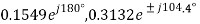
When observing the impulse responses of the continuous and discrete responses, it is hard to miss that they correspond with each other. The analog filter can be represented by a transfer function, Hc(s).
Zeros are the roots of the numerator and poles are the roots of the denominator.
Mapping from s-plane to z-plane
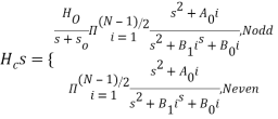
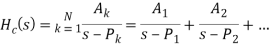
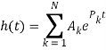
The transfer function of the analog filter in terms of partial fraction expansion with real coefficients is

Where A are the real coefficients and P are the poles of the function And k can be 1, 2 …N.
h(t) is the impulse response of the same analog filter but in the time domain. Since ‘s’ represents a Laplace function Hc(s) can be converted to h(t), by taking its inverse Laplace transform.
Using this transformation,
We obtain

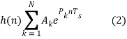
However, in order to obtain a discrete frequency response, we need to sample this equation. Replace ‘nTS’ in the place of t where TS represents the sampling time. This gives us the sampled response h(n),

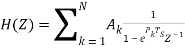
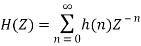
Now, to obtain the transfer function of the IIR Digital Filter which is of the ‘z’ operator, we have to perform z-transform with the newly found sampled impulse response, h(n). For a causal system which depends on past(-n) and current inputs (n), we can get H(z) with the formula shown below

We have already obtained the equation for h(n). Hence, substitute eqn (2) into the above equation
Factoring the coefficient and the common power of n
—(3)
Based on the standard summation formula, (3) is modified and written as the required transfer function of the IIR filter.
 –(4)
–(4)
Hence (4) is obtained from (1), by mapping the poles of the analog filter to that of the digital filter.
That is how you map from the s-plane to z-plane
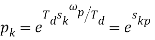
Relationship of S-plane to Z plane
From the equation above, Since, the poles are the denominators we can say  .
.
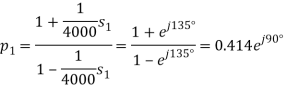
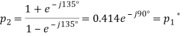
Comparing (1) and (4), we can derive that
 –(5)
–(5)
And since s = PK, substituting into (5) gives us
 –(6)
–(6)
Where
TS is the sampling time
Now, s is taken to be the Laplace operator
 –(7)
–(7)
σ is the attenuation factor
Ω is the analog frequency
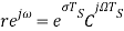
Changing Z from rectangular coordinates to the polar coordinates, we get:
 –(8)
–(8)
Where r is magnitude and ω is digital frequency
Replacing (7) in place of s in (6), and replacing that value as Z in (8)

Compare the real and imaginary parts separately. Where the component with ‘j’ is imaginary.
 –(9)
–(9)
And

Hence, we can make the inference that

To understand the relationship between the s-plane and Z-plane, we need to picture how they will be plotted on a graph. If we were to plot (7) in the ‘s’ domain, σ would be the X-coordinates and jΩ would be the Y-coordinate. Now, if we were to plot (8) in the ‘Z’ domain, the real portion would be the X-coordinate, and the imaginary part would be the Y-coordinate.
Let us take a closer look at equation (9),

There are a few conditions that could help us identify where it is going to be mapped on the s-plane.
Case 1
When σ <0, it would translate that r is the reciprocal of ‘e’ raised to a constant. This will limit the range of r from 0 to 1.
Since σ <0, it would be a negative value and would be mapped on the left-hand side of the graph in the ‘s’ domain
Since 0<r<1, this would fall within the unit circle which has a radius of in the ‘z’ domain.
Case 2
When σ =0, this would make r=e0, which gives us 1, which means r=1. When the radius is 1, it is a unit circle.
Since σ =0, which indicates the Y-axis of the ‘s’ domain.
Since r=1, the point would be on the unit circle in the ‘z’ domain.
Case 3
When σ>0, since it is positive, r would be equal to ‘e’ raised to a particular constant, which means r would also be a positive value greater than 1.
Since σ>0, the positive value would be mapped onto the right-hand side of the ‘s’ domain.
Since r>1, the point would be mapped outside the unit circle in the ‘z’ domain.
Here is a pictorial representation of the three cases:
Mapping of poles located at the imaginary axis of the s-plane onto the unit circle of the z-plane. This is an important condition for accurate transformation.
Mapping of the stable poles on the left-hand side of the imaginary s-plane axis into the unit circle on the z-plane. Poles on the right-hand side of the imaginary axis of the s-plane lie outside the unit circle of the z-plane when mapped.
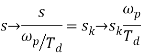
Disadvantages:
- Digital frequency represented by ‘ω,’ and its range lies between – π and π. Analog frequency is represented by ‘Ω,’ and its range lies between – π/TS and π/TS. When mapping from digital to analog, from – π/TS and π/TS , ‘ω’ maps from – π to π. This would make the range of Ω (k-1)π/TS and (k+1)π/TS, where k is an arbitrary constant. However, mapping the other way, from analog to digital, will mean ω maps from – π to π, which makes it many-to-one. Hence, mapping is not one-to-one.
- Analog filters do not have a definite bandwidth because of which when sampling is performed, this would give rise to aliasing. Aliasing is when the signal eats up into the next signal and so on. This would lead to considerable distortion of the signal. Hence, making the frequency response of the converted digital signal very different from the original frequency response of the analog filter.
- Increasing the sampling time will result in a frequency response that is more spaces out hence decreasing the chances of aliasing. However, this is not the case with this method. Increasing the sampling time has no effect on the amount of aliasing that happens.
Key takeaway
The Impulse Invariance Method is used to design a discrete filter that yields a similar frequency response to that of an analog filter. Discrete filters are amazing for two very significant reasons:
- You can separate signals that have been fused and,
- You can use them to retrieve signals that have been distorted.
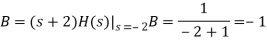
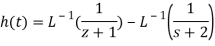
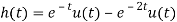
Q. Given  , that has a sampling frequency of 5Hz. Find the transfer function of the IIR digital filter.
Solution:
Step 1:
Step 2:
Applying partial fractions on H(s),


Step 3:

Step 4:

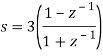
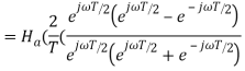
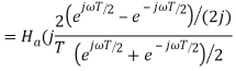
The bilinear transform is the result of a numerical integration of the analog transfer function into the digital domain. We can define the bilinear transform as:

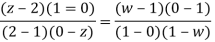
Find the bilinear transformation which maps points z =2,1,0 onto the points w=1,0,i.
Ans. Let, 
And, 
Since bilinear transformation preserves cross ratios,
Thus we have,


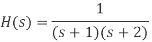
Use the bilinear transformation to convert the analog filtrt with system function

 into a digital IIR filter. Select T =0.1
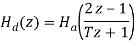
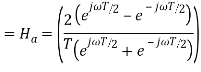
Consider the following system function

Note that the following is the resonant frequency of the analog filter

Consider that the resonant frequency of analog filter must be mapped by selecting the value of parameter
T= 0,1
Use the following mapping for bilinear transformation
Write the system function H(z) of the resultant digital filter

Frequency warping
- The bilinear transformation method has the following important features: A stable analog filter gives a stable digital filter. t The maxima and minima of the amplitude response in the analog filter are preserved in the digital filter. As a consequence, – the pass band ripple, and – the minimum stop band attenuation of the analog filter is preserved in the digital filter frame.
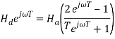
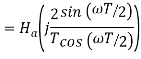
- To determine the frequency response of a continuous-time filter, the transfer function Ha(s)Ha(s) is evaluated at s=jω which is on the jω axis. Likewise, to determine the frequency response of a discrete-time filter, the transfer function Hd(z) is evaluated at z=ejωT which is on the unit circle, |z|=1|z|=1.
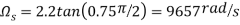
- When the actual frequency of ω is input to the discrete-time filter designed by use of the bilinear transform, it is desired to know at what frequency, ωa, for the continuous-time filter that this ω is mapped to.


- This shows that every point on the unit circle in the discrete-time filter z-plane, z= ejωT is mapped to a point on the jω axis on the continuous-time filter s-plane, s=jω. That is, the discrete-time to continuous-time frequency mapping of the bilinear transform is
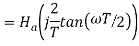
ωa=(2/T) tan(ωt/2)
And the inverse mapping is
ω=(2/T) arc tan(ωaT/2)
- The discrete-time filter behaves at frequency the same way that the continuous-time filter behaves at frequency (2/T)tan(ωT/2). Specifically, the gain and phase shift that the discrete-time filter has at frequency ω is the same gain and phase shift that the continuous-time filter has at frequency (2/T)tan(ωT/2). This means that every feature, every "bump" that is visible in the frequency response of the continuous-time filter is also visible in the discrete-time filter, but at a different frequency. For low frequencies (that is, when ω≪2/T or ωa≪2/T),ω≈ωa.
One can see that the entire continuous frequency range
−∞<ωa<+∞
Is mapped onto the fundamental frequency interval
−πT<ω<+πTω=±π/T.ωa=±∞
One can also see that there is a nonlinear relationship between ωa and ω This effect of the bilinear transform is called frequency warping.

Fig: Frequency Wrapping
Q. Design a discrete time lowpass filter to satisfy the following amplitude specifications: 

Assume 
The pre-warped critical frequency are


Since both the passband and stopband are required to be monotonic, a Butterworth approximation will be used


From the Butterworth design tables we can immediately write

Now find H (z) by first noting that


Using the pole/ zero mapping formula


We can now write

Find  by setting


Finally after multiplying out the numerator and denominator we obtain
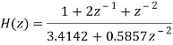
Compare:
Sr No. | Impulse Invariance | Bilinear Transformation |
1 | In this method IIR filters are designed having a unit sample response h (n) that is sampled version of the impulse response of the analog filter. | This method of IIR filter design is based on the trapezoidal formula for numerical integration. |
2 | The bilinear transformation is a conformal mapping that transforms the j  | The bilinear transformation is a conformal mapping tjat transforms the  |
3 | For design of LPF, HPF and almost all types of bandpass and band stop filters this method is used. | For designing of LPF, HPF and almost all types of bandpass and band stop filters this method is used. |
4 | Frequency relationship is non –linear. Frequency warping or frequency compression is due to non – linearity. | Frequency relationship is non linear. Frequency warping or frequency compression is due to non – linearity. |
5 | All poles are mapped from s plane to the z plane by the relationship  | All poles and zeros are mapped. |
At the expense of steepness in transition medium from pass band to stop band this Butterworth filter will provide a flat response in the output signal. So, it is also referred as a maximally flat magnitude filter. The rate of falloff response of the filter is determined by the number of poles taken in the circuit. The pole number will depend on the number of the reactive elements in the circuit that is the number of inductors or capacitors used in the circuits.
The amplitude response of nth order Butterworth filter is given as follows:
Vout / Vin = 1 / √{1 + (f / fc)2n}
Where ‘n’ is the number of poles in the circuit. As the value of the ‘n’ increases the flatness of the filter response also increases.
'f' = operating frequency of the circuit and 'fc' = centre frequency or cut off frequency of the circuit.
These filters have pre-determined considerations whose applications are mainly at active RC circuits at higher frequencies. Even though it does not provide the sharp cut-off response it is often considered as the all-round filter which is used in many applications.
First Order Low Pass Butterworth Filter
The below circuit shows the low pass Butterworth filter:

Fig: First order LP Butterworth Filter
The required pass band gain of the Butterworth filter will mainly depends on the resistor values of ‘R1’ and ‘Rf’ and the cut off frequency of the filter will depend on R and C elements in the above circuit.
The gain of the filter is given as Amax = 1 + (R1 / Rf)
The impedance of the capacitor ‘C’ is given by the -jXC and the voltage across the capacitor is given as,
Vc = - jXC / (R - jXC) * Vin
Where XC = 1 / (2πfc), capacitive Reactance.
The transfer function of the filter in polar form is given as
H(jω) = |Vout/Vin| ∟ø
Where gain of the filter Vout / Vin = Amax / √{1 + (f/fH)²}
And phase angle Ø = - tan-1 ( f/fH )
At lower frequencies means when the operating frequency is lower than the cut-off frequency, the pass band gain is equal to maximum gain.
Vout / Vin = Amax i.e. constant.
At higher frequencies means when the operating frequency is higher than the cut-off frequency, then the gain is less than the maximum gain.
Vout / Vin < Amax
When operating frequency is equal to the cut-off frequency the transfer function is equal to Amax /√2. The rate of decrease in the gain is 20dB/decade or 6dB/octave and can be represented in the response slope as -20dB/decade.
Second Order Low Pass Butterworth Filter
An additional RC network connected to the first order Butterworth filter gives us a second order low pass filter. This second order low pass filter has an advantage that the gain rolls-off very fast after the cut-off frequency, in the stop band.

Fig: Second Order LP Butterworth Filter
In this second order filter, the cut-off frequency value depends on the resistor and capacitor values of two RC sections. The cut-off frequency is calculated using the below formula.
fc = 1 / (2π√R2C2)
The gain rolls off at a rate of 40dB/decade and this response is shown in slope -40dB/decade. The transfer function of the filter can be given as:
Vout / Vin = Amax / √{1 + (f/fc)4}
The standard form of transfer function of the second order filter is given as
Vout / Vin = Amax /s2 + 2εωns + ωn2
Where ωn = natural frequency of oscillations = 1/R2C2
ε = Damping factor = (3 - Amax ) / 2
For second order Butterworth filter, the middle term required is sqrt(2) = 1.414, from the normalized Butterworth polynomial is
3 - Amax = √2 = 1.414
In order to have secured output filter response, it is necessary that the gain Amax is 1.586.
Higher order Butterworth filters are obtained by cascading first and second order Butterworth filters.
n (order) | Normalized Denominator polynomials in factored form |
1 |  |
2 |  |
3 | 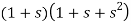 |
The transfer function of the nth order Butterworth filter is given as follows:
H(jω) = 1/√{1 + ε² (ω/ωc)2n}
Where n is the order of the filter
ω is the radian frequency and it is equal to 2πf
And ε is the maximum pass band gain, Amax
Numerical:
Let us consider the Butterworth low pass filter with cut-off frequency 15.9 kHz and with the pass band gain 1.5 and capacitor C = 0.001µF.
fc = 1/2πRC
15.9 * 10³ = 1 / {2πR1 * 0.001 * 10-6}
R = 10kΩ
Amax = 1.5 and assume R1 as 10 kΩ
Amax = 1 + {Rf / R1}
Rf = 5 kΩ
Ideal Frequency Response of the Butterworth Filter
The flatness of the output response increases as the order of the filter increases. The gain and normalized response of the Butterworth filter for different orders are given below:

Fig: Frequency Response of Butterworth Filter
Example. A Butterworth Amplitude Response design
Let, 
Solving for N gives


Matching at 
The normal  from the table is

Frequency seal  impliea that we let
Finally, the frequency scaled system function is

A Chebyshev design achieves a more rapid roll-off rate near the cut-off frequency than the Butterworth by allowing ripple in the passband (type I) or stopband (type II). Monotonicity of the stopband or passband is still maintained respectively.

Fig: Chebyshev Filter Type I and II
Chebyshev Type I
The magnitude response is given by

Where,
 Nth order Chebyshev polynomial
And  specifies the passband ripple
The Chebyshev polynomials are of the form\

With recurrence formula

An alternate form for  which will be useful in both analysis and design is

Design a Chebyshev type I lowpass filter to satisfy the following amplitude specification 
Using the design formula for N

From the 2dB ripple table (9-20)
Elliptic Design
Allows both passband and stopband ripple to obtain a narrow transition band. The elliptic (Cauer) filter is optimum in the sense that no other filter of the same order can provide a narrower transition band.
The squared magnitude response is given by
Define the transition region ratio as

The normalized lowpass system function can be written in factored form as

Note:  contains conjugate pairs of zeros on the j
 axis which give the stopband nulls.
The filter coefficients  if N is odd.
Design an elliptic lowpass filter to satisfy the following amplitude specifications, 

From the 1dB ripple, 40Db stopband attenuation table wew find that N meets or exceeds the
  = 1.2187, so we can scale
  and then the desired stopband attenuation will actually be achieved at
  .
.
T6he normalized H (z)  is
is
H(s)=(0.046998s4+0.22007s2+0.22985)/(s5+0.92339s4+1.84712s3+1.12923s2+0.78813s
To complete the design scale H (s) by letting 
Example. Design from a Rational H (s)
Let, 
Inverse Laplace transforming yields
Sampling  seconds and gain scaling we obtain
Which implies that
Setting  requires that

Q. Design a Chebyshev type 1 low pass filter to satisfy the following amplitude specifications: 
Using the design formula for N
N = [2.08]=3
Note: 
The normalized system function is
With poles at
To frequency scale  let
let

So in the z domain

Note that when the design originates from discrete time specifications the poles of H (z) are independent of  .
.
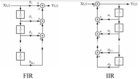
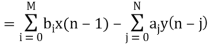
Direct form I
The difference equation


Specifies the Direct-Form I (DF-I) implementation of a digital filter. The DF-I signal flow graph for the second-order case is shown in Fig.

Figure: Direct-Form-I implementation of a 2nd-order digital filter.
Direct form II
The signal flow graph for the Direct-Form-II (DF-II) realization of the second-order IIR filter section is shown in Fig.
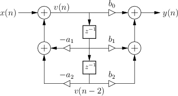
Figure: Direct-Form-II implementation of a 2nd-order digital filter.
The difference equation for the second-order DF-II structure can be written as


Which can be interpreted as a two-pole filter followed in series by a two-zero filter.
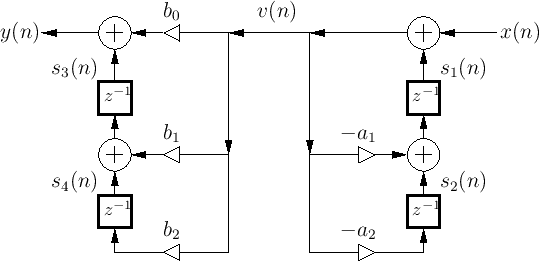
Fig. Transposed-Direct-Form-I

Fig. Transposed-Direct-Form-II implementation of a second-order IIR digital filter
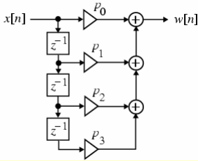
The filter section can be seen to be an FIR filter and can be realized as shown below
W[n] = p0x[n] + p1x[n-1] + p2x[n-2] +p3x[n-3]

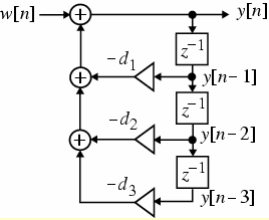
The time-domain representation of H2(z) is given by
Y[n] = w[n] –d1y[n-1] –d2y[n-2] – d3y[n-3]

A cascade of the two structures realizing and leads to the realization of shown below and is known as the direct form I structure

Fig: Cascade form
Direct form II and cascade form realizations of

Fig: Direct form II

Fig: Cascade form
The parallel form is obtained from

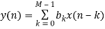
Based on the above equation, we need the current input sample and M−1 previous samples of the input to produce an output point. For M=5, we can simply obtain the following diagram from Equation 1.

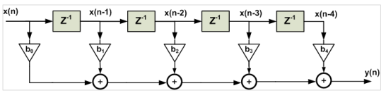
On the other hand, for a linear-phase FIR filter, we observe the following symmetry in coefficients of the difference equation
The structure obtained from the above equation is shown in Figure 2. While Figure 1 requires five multipliers, employing the symmetry of a linear-phase FIR filter, we can implement the filter using only three multipliers. This example shows that for an odd M, the symmetry property reduces the number of multipliers of an (M−1)th-order FIR filter from M to M+1/2.

Example. A partial fraction expansion of


The corresponding parallel form I realization is shown below
Lattice IIR Structure
Consider a system with finite poles and all its zeros at z = 0 whose transfer function is of the form
H(z) = 
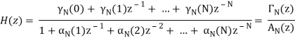
Where AN(z) = 1 +  is an Nth degree polynomial in z. This system has N finite poles and N zeros at z = 0.
Lattice IIR Direct form II Structure
A Direct Form II system with N finite poles and N zeros at z = 0.

Fig. Lattice IIR Structure
Comparison of Direct Form II structures for FIR and IIR systems.
If, in the FIR system, we exchange the roles of X (z) and Y (z),change allb's to -a's (with b0 = 1) and let N = M - 1, we get theIIR system.
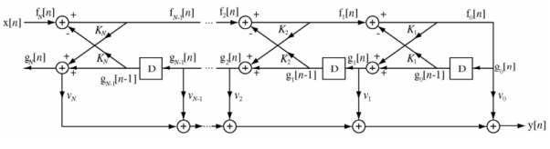
Modify the FIR lattice structure as illustrated below. Reverse the arrows on all the "f" signals. Reverse the lattice and apply x [n] to the previous output and take y [n] from the previous input.
Also reverse the signs of the signals arriving from the bottom. This is now a recursive or feedback structure which can implement an IIR filter.

Fig. Lattice-Ladder IIR Structure
Take the case N = 1
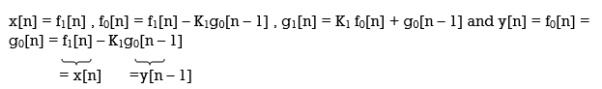
z transforming
Y(z) + K1z-1Y(z) = X(z) H1(z) = 
Single pole at z = - K1 and a zero at z = 0.

Fig. Lattice-Ladder IIR Structure
Also, for the N = 1 case
g1[n] = K1y[n] + y[n – 1]
G1(z) = K1Y(z) + z-1Y(z) G1(z)/Y(z) = K1 + z-1 = K1 
G1(z)/Y(z) is the transfer function of a system with a single zero at
z = -1/K1 and a pole at zero.
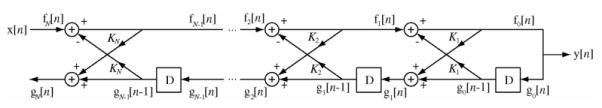
Fig. Lattice-Ladder IIR Structure
For the N = 2 case, it can be shown that
H2(z) = Y(z)/X(z) = 
And
G2(z)/Y(z) = K2 + K1(K2 + 1)z-1 + z-2 = K2 
Notice that the coefficients for the FIR and IIR systems occur in reverse order as before.

Fig. Lattice-Ladder IIR Structure
For any m,
Hm(z) = Y(z)/X(z) = 1/Am(z) and Gm(z)/Y(z) = Bm (z) = z-mAm(1/z)
And the previous relations for FIR lattices still hold.
A0(z) = B0(z) = 1, Am(z) = Am-1(z) + Kmz-1Bm-1(z)
Bm(z) = z-m Am(1/z), Km αm[m]


Fig. Lattice-Ladder IIR Structure
If we want to add finite zeros to Hm(z) we can add a ladder network to the lattice. Then the transfer function will be of the form.

y[n] = 

Lattice-Ladder Example
Synthesize the transfer function

Using a lattice-ladder network.
A2(z) = 1+ 0.2z-1 – 0.15 z-2
K2 = -0.15 and B2(z) = -0.15 + 0.2z-1 + z-2
Γ2(z) =  - z-1 + 0.5z-2 v2 = 0.5
Γ1(z) = Γ2(z) – v2B2(z) = 1 – z-1 + 0.5z-2 – 0.5 (- 0.15 + 0.2z-1 + z-2)
Γ1(z) = 1,075 – 1.1z-1 v1 = - 1.1
Γ0(z) = Γ1(z) – v1B1(z)
Lattice-Ladder Example
Using Am-1(z) = 
A1(z) = 
A1(z) = 
K1 = 0.23529 and B1(z) = 0.23529 + z-1
Γ0(z) = 1.075 – 1.1z-1 – (-1.1)(0.23529 + z-1) = 1.3382 v0 = 1.3382

References:
1. Digital signal processing- A practical approach Second Edition, 2002.E. C. Ifeachar, B. W. Jarvis Pearson Education
2. Sanjit K. Mitra, ‘Digital Signal Processing – A Computer based approach’
3. S. Salivahanan, A Vallavaraj, C. Gnanapriya, ‘Digital Signal Processing’, 2nd Edition McGraw Hill.
4. A. Nagoor Kani, ‘Digital Signal Processing’, 2nd Edition McGraw Hill.
5. P. Ramesh Babu, ‘Digital Signal Processing’ Scitech
Unit - 4
IIR Filter Design & Realization
Filters are networks that process signals in a frequency-dependent manner. The basic concept of a filter can be explained by examining the frequency dependent nature of the impedance of capacitors and inductors. Consider a voltage divider where the shunt leg is a reactive impedance.
As the frequency is changed, the value of the reactive impedance changes, and the voltage divider ratio changes. This mechanism yields the frequency dependent change in the input/output transfer function that is defined as the frequency response.
A simple, single-pole, high-pass filter can be used to block dc offset in high gain amplifiers or single supply circuits. Filters can be used to separate signals, passing those of interest, and attenuating the unwanted frequencies.
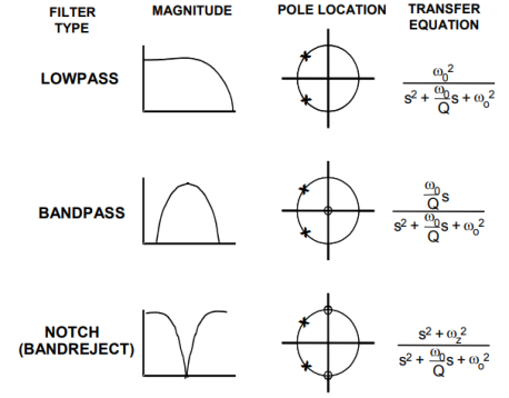

Fig: Basic Analog Filters
Key takeaway
Sr. No | Analog filter | Digital filter |
1. | Analog filters are used for filtering analog signals. | Digital filters are used for filtering digital sequences |
2. | Analog filters are designed with various components like resistor, inductor and capacitor. | Digital filters are designed with digital hardware like FF, counters shift registers, ALU and software’s like C or assemble language. |
3 | Analog filters less accurate and because of component tolerance of active components and more sensitive to environmental changes | Digital filters are less sensitive to the environmental changes, noise and disturbances. Thus periodic calibration can be avoided. Also they are extremely stable. |
4. | Less flexible | These are most flexible as software programs & control programs can be easily modified. Several input signals can be filtered by one digital filter. |
5. | Filter representation is in terms of system components | Digital filters are represented by the difference equation. |
6 | An analog filter can only be change by redesigning the filter circuit. | A digital is programmable ie its operation is determined by a program stored in the processor’s memory. This means the digital filter can easily be changed without affecting the circuitry (hardware). |
Consider an analog filter. It’s transfer function will be of the differential equation form as shown below.

Taking Laplace transform on both ends:

The transfer function of the analog filter can be given by:
Note that this is just a generic transfer function. To get the transfer function of a digital filter we will dive into some specifics.

Thus,
Taking z-transform on both sides:

Solving for the transfer function of the digital filter:

The mapping between S and Z planes
To map from s to z-plane we need to find the values of σ and Ω in s = σ + jΩ. We have the relationship between s and z from above as:

Rewriting the above equation for z:

Substituting s = σ+jΩ in the above equation and solving gives us:

Separating the real and imaginary parts we get:
For σ=0
When we vary Ω from -∞ to +∞, the corresponding locus of points in the z-plane is a circle with radius 1/2 and with its center at z=1/2.
Similarly, when we map the equation  the left half-plane of the s-domain maps inside the circle with 0.5 radians. Moreover, the right half-plane of the s-domain is mapped outside the unit circle.

Fig: Mapping of S and z-plane
Mapping of s-plane into the z-plane by the approximation of derivatives method.
Thus, we can say that this transformation of an analog filter results in a stable digital filter.
Limitations:
From the above fig, the location of poles in the z-domain is confined to smaller frequencies. Thus the approximation of derivatives method is limited to designing low pass and bandpass IIR filters with small resonant frequencies only. It can’t be used to develop high pass and band-reject filters.
Key takeaway
From the above fig, the location of poles in the z-domain is confined to smaller frequencies. Thus, the approximation of derivatives method is limited to designing low pass and bandpass IIR filters with small resonant frequencies only. It can’t be used to develop high pass and band-reject filters.
Numerical:
Q. Design a Discrete Time Low Pass Filter for a voice signal. The specifications are: Passband Fp 4 kHz, with 0.8 dB ripple; Stopband FS 4.5 kHz, with 50dB attenuation; Sampling Frequency Fs 22 kHz. Determine a) the discrete time Passband and Stopband frequencies, b) the maximum and minimum values of H () in the Passband and the Stopband, where () is the filter frequency response.
Solution
a) Recall the mapping from analog to digital frequency 2 F/Fs , with Fs the sampling frequency. Then the passband and stopband frequencies become p 2 4/ 22 rad 0.36 rad, s 2 4.5/ 22 rad 0.41 rad;
b) A 0.8 dB ripple means that the frequency response in the passband is within the interval 1 where is such that 20 log10 (1+) 0.8 This yields 100.04 1 0.096.
Therefore the frequency response within the passband is within the interval 0.9035 H() 1.096. Similarly in the stopband the maximum value is () 1050/20 0.0031
The Impulse Invariance Method is used to design a discrete filter that yields a similar frequency response to that of an analog filter. Discrete filters are amazing for two very significant reasons:
- You can separate signals that have been fused and,
- You can use them to retrieve signals that have been distorted.
We can design this filter by finding out one very important piece of information i.e., the impulse response of the analog filter. By sampling the response we will get the time-domain impulse response of the discrete filter.
When observing the impulse responses of the continuous and discrete responses, it is hard to miss that they correspond with each other. The analog filter can be represented by a transfer function, Hc(s).
Zeros are the roots of the numerator and poles are the roots of the denominator.
Mapping from s-plane to z-plane
The transfer function of the analog filter in terms of partial fraction expansion with real coefficients is

Where A are the real coefficients and P are the poles of the function And k can be 1, 2 …N.
h(t) is the impulse response of the same analog filter but in the time domain. Since ‘s’ represents a Laplace function Hc(s) can be converted to h(t), by taking its inverse Laplace transform.
Using this transformation,
We obtain

However, in order to obtain a discrete frequency response, we need to sample this equation. Replace ‘nTS’ in the place of t where TS represents the sampling time. This gives us the sampled response h(n),
Now, to obtain the transfer function of the IIR Digital Filter which is of the ‘z’ operator, we have to perform z-transform with the newly found sampled impulse response, h(n). For a causal system which depends on past(-n) and current inputs (n), we can get H(z) with the formula shown below

We have already obtained the equation for h(n). Hence, substitute eqn (2) into the above equation
Factoring the coefficient and the common power of n
—(3)
Based on the standard summation formula, (3) is modified and written as the required transfer function of the IIR filter.
 –(4)
–(4)
Hence (4) is obtained from (1), by mapping the poles of the analog filter to that of the digital filter.

That is how you map from the s-plane to z-plane
Relationship of S-plane to Z plane
From the equation above, Since, the poles are the denominators we can say  .
.
Comparing (1) and (4), we can derive that
 –(5)
–(5)
And since s = PK, substituting into (5) gives us
 –(6)
–(6)
Where
TS is the sampling time
Now, s is taken to be the Laplace operator
 –(7)
–(7)
σ is the attenuation factor
Ω is the analog frequency
Changing Z from rectangular coordinates to the polar coordinates, we get:
 –(8)
–(8)
Where r is magnitude and ω is digital frequency
Replacing (7) in place of s in (6), and replacing that value as Z in (8)


Compare the real and imaginary parts separately. Where the component with ‘j’ is imaginary.
 –(9)
–(9)
And

Hence, we can make the inference that

To understand the relationship between the s-plane and Z-plane, we need to picture how they will be plotted on a graph. If we were to plot (7) in the ‘s’ domain, σ would be the X-coordinates and jΩ would be the Y-coordinate. Now, if we were to plot (8) in the ‘Z’ domain, the real portion would be the X-coordinate, and the imaginary part would be the Y-coordinate.
Let us take a closer look at equation (9),

There are a few conditions that could help us identify where it is going to be mapped on the s-plane.
Case 1
When σ <0, it would translate that r is the reciprocal of ‘e’ raised to a constant. This will limit the range of r from 0 to 1.
Since σ <0, it would be a negative value and would be mapped on the left-hand side of the graph in the ‘s’ domain
Since 0<r<1, this would fall within the unit circle which has a radius of in the ‘z’ domain.
Case 2
When σ =0, this would make r=e0, which gives us 1, which means r=1. When the radius is 1, it is a unit circle.
Since σ =0, which indicates the Y-axis of the ‘s’ domain.
Since r=1, the point would be on the unit circle in the ‘z’ domain.
Case 3
When σ>0, since it is positive, r would be equal to ‘e’ raised to a particular constant, which means r would also be a positive value greater than 1.
Since σ>0, the positive value would be mapped onto the right-hand side of the ‘s’ domain.
Since r>1, the point would be mapped outside the unit circle in the ‘z’ domain.
Here is a pictorial representation of the three cases:

Mapping of poles located at the imaginary axis of the s-plane onto the unit circle of the z-plane. This is an important condition for accurate transformation.

Mapping of the stable poles on the left-hand side of the imaginary s-plane axis into the unit circle on the z-plane. Poles on the right-hand side of the imaginary axis of the s-plane lie outside the unit circle of the z-plane when mapped.
Disadvantages:
- Digital frequency represented by ‘ω,’ and its range lies between – π and π. Analog frequency is represented by ‘Ω,’ and its range lies between – π/TS and π/TS. When mapping from digital to analog, from – π/TS and π/TS , ‘ω’ maps from – π to π. This would make the range of Ω (k-1)π/TS and (k+1)π/TS, where k is an arbitrary constant. However, mapping the other way, from analog to digital, will mean ω maps from – π to π, which makes it many-to-one. Hence, mapping is not one-to-one.
- Analog filters do not have a definite bandwidth because of which when sampling is performed, this would give rise to aliasing. Aliasing is when the signal eats up into the next signal and so on. This would lead to considerable distortion of the signal. Hence, making the frequency response of the converted digital signal very different from the original frequency response of the analog filter.
- Increasing the sampling time will result in a frequency response that is more spaces out hence decreasing the chances of aliasing. However, this is not the case with this method. Increasing the sampling time has no effect on the amount of aliasing that happens.
Key takeaway
The Impulse Invariance Method is used to design a discrete filter that yields a similar frequency response to that of an analog filter. Discrete filters are amazing for two very significant reasons:
- You can separate signals that have been fused and,
- You can use them to retrieve signals that have been distorted.
Q. Given  , that has a sampling frequency of 5Hz. Find the transfer function of the IIR digital filter.
Solution:
Step 1:

Step 2:
Applying partial fractions on H(s),


Step 3:

Step 4:

The bilinear transform is the result of a numerical integration of the analog transfer function into the digital domain. We can define the bilinear transform as:

Find the bilinear transformation which maps points z =2,1,0 onto the points w=1,0,i.
Ans. Let, 
And, 
Since bilinear transformation preserves cross ratios,
Thus we have,


Use the bilinear transformation to convert the analog filtrt with system function

 into a digital IIR filter. Select T =0.1
Consider the following system function

Note that the following is the resonant frequency of the analog filter

Consider that the resonant frequency of analog filter must be mapped by selecting the value of parameter
T= 0,1
Use the following mapping for bilinear transformation

Write the system function H(z) of the resultant digital filter

Frequency warping
- The bilinear transformation method has the following important features: A stable analog filter gives a stable digital filter. t The maxima and minima of the amplitude response in the analog filter are preserved in the digital filter. As a consequence, – the pass band ripple, and – the minimum stop band attenuation of the analog filter is preserved in the digital filter frame.
- To determine the frequency response of a continuous-time filter, the transfer function Ha(s)Ha(s) is evaluated at s=jω which is on the jω axis. Likewise, to determine the frequency response of a discrete-time filter, the transfer function Hd(z) is evaluated at z=ejωT which is on the unit circle, |z|=1|z|=1.
- When the actual frequency of ω is input to the discrete-time filter designed by use of the bilinear transform, it is desired to know at what frequency, ωa, for the continuous-time filter that this ω is mapped to.


- This shows that every point on the unit circle in the discrete-time filter z-plane, z= ejωT is mapped to a point on the jω axis on the continuous-time filter s-plane, s=jω. That is, the discrete-time to continuous-time frequency mapping of the bilinear transform is
ωa=(2/T) tan(ωt/2)
And the inverse mapping is
ω=(2/T) arc tan(ωaT/2)
- The discrete-time filter behaves at frequency the same way that the continuous-time filter behaves at frequency (2/T)tan(ωT/2). Specifically, the gain and phase shift that the discrete-time filter has at frequency ω is the same gain and phase shift that the continuous-time filter has at frequency (2/T)tan(ωT/2). This means that every feature, every "bump" that is visible in the frequency response of the continuous-time filter is also visible in the discrete-time filter, but at a different frequency. For low frequencies (that is, when ω≪2/T or ωa≪2/T),ω≈ωa.
One can see that the entire continuous frequency range
−∞<ωa<+∞
Is mapped onto the fundamental frequency interval
−πT<ω<+πTω=±π/T.ωa=±∞
One can also see that there is a nonlinear relationship between ωa and ω This effect of the bilinear transform is called frequency warping.
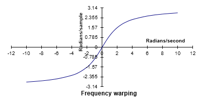
Fig: Frequency Wrapping
Q. Design a discrete time lowpass filter to satisfy the following amplitude specifications: 

Assume 
The pre-warped critical frequency are
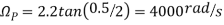


Since both the passband and stopband are required to be monotonic, a Butterworth approximation will be used

From the Butterworth design tables we can immediately write
Now find H (z) by first noting that

Using the pole/ zero mapping formula


We can now write

Find  by setting
Finally after multiplying out the numerator and denominator we obtain

Compare:
Sr No. | Impulse Invariance | Bilinear Transformation |
1 | In this method IIR filters are designed having a unit sample response h (n) that is sampled version of the impulse response of the analog filter. | This method of IIR filter design is based on the trapezoidal formula for numerical integration. |
2 | The bilinear transformation is a conformal mapping that transforms the j  | The bilinear transformation is a conformal mapping tjat transforms the  |
3 | For design of LPF, HPF and almost all types of bandpass and band stop filters this method is used. | For designing of LPF, HPF and almost all types of bandpass and band stop filters this method is used. |
4 | Frequency relationship is non –linear. Frequency warping or frequency compression is due to non – linearity. | Frequency relationship is non linear. Frequency warping or frequency compression is due to non – linearity. |
5 | All poles are mapped from s plane to the z plane by the relationship  | All poles and zeros are mapped. |
At the expense of steepness in transition medium from pass band to stop band this Butterworth filter will provide a flat response in the output signal. So, it is also referred as a maximally flat magnitude filter. The rate of falloff response of the filter is determined by the number of poles taken in the circuit. The pole number will depend on the number of the reactive elements in the circuit that is the number of inductors or capacitors used in the circuits.
The amplitude response of nth order Butterworth filter is given as follows:
Vout / Vin = 1 / √{1 + (f / fc)2n}
Where ‘n’ is the number of poles in the circuit. As the value of the ‘n’ increases the flatness of the filter response also increases.
'f' = operating frequency of the circuit and 'fc' = centre frequency or cut off frequency of the circuit.
These filters have pre-determined considerations whose applications are mainly at active RC circuits at higher frequencies. Even though it does not provide the sharp cut-off response it is often considered as the all-round filter which is used in many applications.
First Order Low Pass Butterworth Filter
The below circuit shows the low pass Butterworth filter:

Fig: First order LP Butterworth Filter
The required pass band gain of the Butterworth filter will mainly depends on the resistor values of ‘R1’ and ‘Rf’ and the cut off frequency of the filter will depend on R and C elements in the above circuit.
The gain of the filter is given as Amax = 1 + (R1 / Rf)
The impedance of the capacitor ‘C’ is given by the -jXC and the voltage across the capacitor is given as,
Vc = - jXC / (R - jXC) * Vin
Where XC = 1 / (2πfc), capacitive Reactance.
The transfer function of the filter in polar form is given as
H(jω) = |Vout/Vin| ∟ø
Where gain of the filter Vout / Vin = Amax / √{1 + (f/fH)²}
And phase angle Ø = - tan-1 ( f/fH )
At lower frequencies means when the operating frequency is lower than the cut-off frequency, the pass band gain is equal to maximum gain.
Vout / Vin = Amax i.e. constant.
At higher frequencies means when the operating frequency is higher than the cut-off frequency, then the gain is less than the maximum gain.
Vout / Vin < Amax
When operating frequency is equal to the cut-off frequency the transfer function is equal to Amax /√2. The rate of decrease in the gain is 20dB/decade or 6dB/octave and can be represented in the response slope as -20dB/decade.
Second Order Low Pass Butterworth Filter
An additional RC network connected to the first order Butterworth filter gives us a second order low pass filter. This second order low pass filter has an advantage that the gain rolls-off very fast after the cut-off frequency, in the stop band.
Fig: Second Order LP Butterworth Filter
In this second order filter, the cut-off frequency value depends on the resistor and capacitor values of two RC sections. The cut-off frequency is calculated using the below formula.
fc = 1 / (2π√R2C2)
The gain rolls off at a rate of 40dB/decade and this response is shown in slope -40dB/decade. The transfer function of the filter can be given as:
Vout / Vin = Amax / √{1 + (f/fc)4}
The standard form of transfer function of the second order filter is given as
Vout / Vin = Amax /s2 + 2εωns + ωn2
Where ωn = natural frequency of oscillations = 1/R2C2
ε = Damping factor = (3 - Amax ) / 2
For second order Butterworth filter, the middle term required is sqrt(2) = 1.414, from the normalized Butterworth polynomial is
3 - Amax = √2 = 1.414
In order to have secured output filter response, it is necessary that the gain Amax is 1.586.
Higher order Butterworth filters are obtained by cascading first and second order Butterworth filters.
n (order) | Normalized Denominator polynomials in factored form |
1 |  |
2 |  |
3 |  |
The transfer function of the nth order Butterworth filter is given as follows:
H(jω) = 1/√{1 + ε² (ω/ωc)2n}
Where n is the order of the filter
ω is the radian frequency and it is equal to 2πf
And ε is the maximum pass band gain, Amax
Numerical:
Let us consider the Butterworth low pass filter with cut-off frequency 15.9 kHz and with the pass band gain 1.5 and capacitor C = 0.001µF.
fc = 1/2πRC
15.9 * 10³ = 1 / {2πR1 * 0.001 * 10-6}
R = 10kΩ
Amax = 1.5 and assume R1 as 10 kΩ
Amax = 1 + {Rf / R1}
Rf = 5 kΩ

Ideal Frequency Response of the Butterworth Filter
The flatness of the output response increases as the order of the filter increases. The gain and normalized response of the Butterworth filter for different orders are given below:
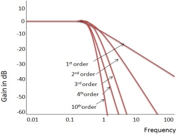
Fig: Frequency Response of Butterworth Filter
Example. A Butterworth Amplitude Response design
Let, 

Solving for N gives

Matching at 

The normal  from the table is

Frequency seal  impliea that we let
Finally, the frequency scaled system function is
A Chebyshev design achieves a more rapid roll-off rate near the cut-off frequency than the Butterworth by allowing ripple in the passband (type I) or stopband (type II). Monotonicity of the stopband or passband is still maintained respectively.
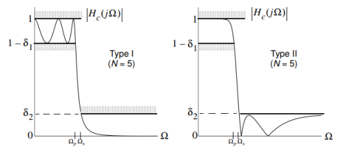
Fig: Chebyshev Filter Type I and II
Chebyshev Type I
The magnitude response is given by
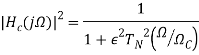
Where,
 Nth order Chebyshev polynomial
And  specifies the passband ripple
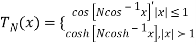
The Chebyshev polynomials are of the form\

With recurrence formula

An alternate form for  which will be useful in both analysis and design is
Design a Chebyshev type I lowpass filter to satisfy the following amplitude specification 
Using the design formula for N

From the 2dB ripple table (9-20)

Elliptic Design
Allows both passband and stopband ripple to obtain a narrow transition band. The elliptic (Cauer) filter is optimum in the sense that no other filter of the same order can provide a narrower transition band.
The squared magnitude response is given by


Define the transition region ratio as

The normalized lowpass system function can be written in factored form as
Note:  contains conjugate pairs of zeros on the j
 axis which give the stopband nulls.
The filter coefficients  if N is odd.
Design an elliptic lowpass filter to satisfy the following amplitude specifications, 

From the 1dB ripple, 40Db stopband attenuation table wew find that N meets or exceeds the
  = 1.2187, so we can scale
  and then the desired stopband attenuation will actually be achieved at
  .
.
T6he normalized H (z)  is
is
H(s)=(0.046998s4+0.22007s2+0.22985)/(s5+0.92339s4+1.84712s3+1.12923s2+0.78813s
To complete the design scale H (s) by letting 
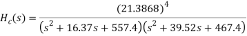
Example. Design from a Rational H (s)
Let, 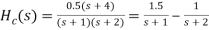
Inverse Laplace transforming yields

Sampling  seconds and gain scaling we obtain

Which implies that

Setting  requires that

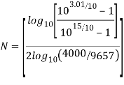
Q. Design a Chebyshev type 1 low pass filter to satisfy the following amplitude specifications: 
Using the design formula for N
N = [2.08]=3
Note: 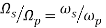
The normalized system function is

With poles at

To frequency scale  let
let
So in the z domain
Note that when the design originates from discrete time specifications the poles of H (z) are independent of  .
.
Direct form I
The difference equation


Specifies the Direct-Form I (DF-I) implementation of a digital filter. The DF-I signal flow graph for the second-order case is shown in Fig.
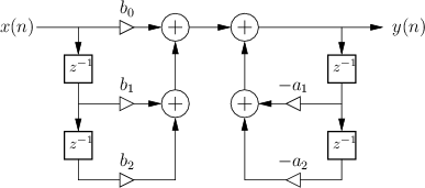
Figure: Direct-Form-I implementation of a 2nd-order digital filter.
Direct form II
The signal flow graph for the Direct-Form-II (DF-II) realization of the second-order IIR filter section is shown in Fig.

Figure: Direct-Form-II implementation of a 2nd-order digital filter.
The difference equation for the second-order DF-II structure can be written as


Which can be interpreted as a two-pole filter followed in series by a two-zero filter.

Fig. Transposed-Direct-Form-I
Fig. Transposed-Direct-Form-II implementation of a second-order IIR digital filter
The filter section can be seen to be an FIR filter and can be realized as shown below
W[n] = p0x[n] + p1x[n-1] + p2x[n-2] +p3x[n-3]
The time-domain representation of H2(z) is given by
Y[n] = w[n] –d1y[n-1] –d2y[n-2] – d3y[n-3]
A cascade of the two structures realizing and leads to the realization of shown below and is known as the direct form I structure
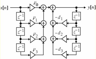
Fig: Cascade form
Direct form II and cascade form realizations of
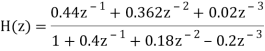


Fig: Direct form II
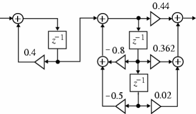
Fig: Cascade form
The parallel form is obtained from
Based on the above equation, we need the current input sample and M−1 previous samples of the input to produce an output point. For M=5, we can simply obtain the following diagram from Equation 1.
On the other hand, for a linear-phase FIR filter, we observe the following symmetry in coefficients of the difference equation
The structure obtained from the above equation is shown in Figure 2. While Figure 1 requires five multipliers, employing the symmetry of a linear-phase FIR filter, we can implement the filter using only three multipliers. This example shows that for an odd M, the symmetry property reduces the number of multipliers of an (M−1)th-order FIR filter from M to M+1/2.
Example. A partial fraction expansion of


The corresponding parallel form I realization is shown below

Lattice IIR Structure
Consider a system with finite poles and all its zeros at z = 0 whose transfer function is of the form
H(z) = 
Where AN(z) = 1 + 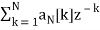 is an Nth degree polynomial in z. This system has N finite poles and N zeros at z = 0.
Lattice IIR Direct form II Structure
A Direct Form II system with N finite poles and N zeros at z = 0.

Fig. Lattice IIR Structure
Comparison of Direct Form II structures for FIR and IIR systems.
If, in the FIR system, we exchange the roles of X (z) and Y (z),change allb's to -a's (with b0 = 1) and let N = M - 1, we get theIIR system.

Modify the FIR lattice structure as illustrated below. Reverse the arrows on all the "f" signals. Reverse the lattice and apply x [n] to the previous output and take y [n] from the previous input.
Also reverse the signs of the signals arriving from the bottom. This is now a recursive or feedback structure which can implement an IIR filter.
Fig. Lattice-Ladder IIR Structure
Take the case N = 1

z transforming
Y(z) + K1z-1Y(z) = X(z) H1(z) = 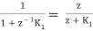
Single pole at z = - K1 and a zero at z = 0.
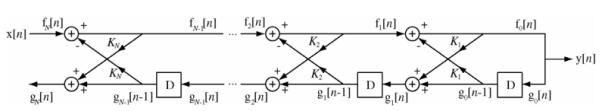
Fig. Lattice-Ladder IIR Structure
Also, for the N = 1 case
g1[n] = K1y[n] + y[n – 1]
G1(z) = K1Y(z) + z-1Y(z) G1(z)/Y(z) = K1 + z-1 = K1 
G1(z)/Y(z) is the transfer function of a system with a single zero at
z = -1/K1 and a pole at zero.

Fig. Lattice-Ladder IIR Structure
For the N = 2 case, it can be shown that
H2(z) = Y(z)/X(z) = 
And
G2(z)/Y(z) = K2 + K1(K2 + 1)z-1 + z-2 = K2 
Notice that the coefficients for the FIR and IIR systems occur in reverse order as before.

Fig. Lattice-Ladder IIR Structure
For any m,
Hm(z) = Y(z)/X(z) = 1/Am(z) and Gm(z)/Y(z) = Bm (z) = z-mAm(1/z)
And the previous relations for FIR lattices still hold.
A0(z) = B0(z) = 1, Am(z) = Am-1(z) + Kmz-1Bm-1(z)
Bm(z) = z-m Am(1/z), Km αm[m]

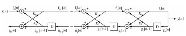
Fig. Lattice-Ladder IIR Structure
If we want to add finite zeros to Hm(z) we can add a ladder network to the lattice. Then the transfer function will be of the form.
y[n] = 
Lattice-Ladder Example
Synthesize the transfer function

Using a lattice-ladder network.
A2(z) = 1+ 0.2z-1 – 0.15 z-2
K2 = -0.15 and B2(z) = -0.15 + 0.2z-1 + z-2
Γ2(z) =  - z-1 + 0.5z-2 v2 = 0.5
Γ1(z) = Γ2(z) – v2B2(z) = 1 – z-1 + 0.5z-2 – 0.5 (- 0.15 + 0.2z-1 + z-2)
Γ1(z) = 1,075 – 1.1z-1 v1 = - 1.1
Γ0(z) = Γ1(z) – v1B1(z)
Lattice-Ladder Example
Using Am-1(z) = 
A1(z) = 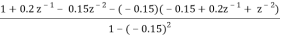
A1(z) = 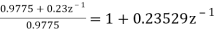
K1 = 0.23529 and B1(z) = 0.23529 + z-1
Γ0(z) = 1.075 – 1.1z-1 – (-1.1)(0.23529 + z-1) = 1.3382 v0 = 1.3382

References:
1. Digital signal processing- A practical approach Second Edition, 2002.E. C. Ifeachar, B. W. Jarvis Pearson Education
2. Sanjit K. Mitra, ‘Digital Signal Processing – A Computer based approach’
3. S. Salivahanan, A Vallavaraj, C. Gnanapriya, ‘Digital Signal Processing’, 2nd Edition McGraw Hill.
4. A. Nagoor Kani, ‘Digital Signal Processing’, 2nd Edition McGraw Hill.
5. P. Ramesh Babu, ‘Digital Signal Processing’ Scitech
Unit - 4
IIR Filter Design & Realization
Filters are networks that process signals in a frequency-dependent manner. The basic concept of a filter can be explained by examining the frequency dependent nature of the impedance of capacitors and inductors. Consider a voltage divider where the shunt leg is a reactive impedance.
As the frequency is changed, the value of the reactive impedance changes, and the voltage divider ratio changes. This mechanism yields the frequency dependent change in the input/output transfer function that is defined as the frequency response.
A simple, single-pole, high-pass filter can be used to block dc offset in high gain amplifiers or single supply circuits. Filters can be used to separate signals, passing those of interest, and attenuating the unwanted frequencies.

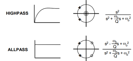
Fig: Basic Analog Filters
Key takeaway
Sr. No | Analog filter | Digital filter |
1. | Analog filters are used for filtering analog signals. | Digital filters are used for filtering digital sequences |
2. | Analog filters are designed with various components like resistor, inductor and capacitor. | Digital filters are designed with digital hardware like FF, counters shift registers, ALU and software’s like C or assemble language. |
3 | Analog filters less accurate and because of component tolerance of active components and more sensitive to environmental changes | Digital filters are less sensitive to the environmental changes, noise and disturbances. Thus periodic calibration can be avoided. Also they are extremely stable. |
4. | Less flexible | These are most flexible as software programs & control programs can be easily modified. Several input signals can be filtered by one digital filter. |
5. | Filter representation is in terms of system components | Digital filters are represented by the difference equation. |
6 | An analog filter can only be change by redesigning the filter circuit. | A digital is programmable ie its operation is determined by a program stored in the processor’s memory. This means the digital filter can easily be changed without affecting the circuitry (hardware). |
Consider an analog filter. It’s transfer function will be of the differential equation form as shown below.

Taking Laplace transform on both ends:

The transfer function of the analog filter can be given by:

Note that this is just a generic transfer function. To get the transfer function of a digital filter we will dive into some specifics.

Thus,

Taking z-transform on both sides:

Solving for the transfer function of the digital filter:

The mapping between S and Z planes
To map from s to z-plane we need to find the values of σ and Ω in s = σ + jΩ. We have the relationship between s and z from above as:

Rewriting the above equation for z:

Substituting s = σ+jΩ in the above equation and solving gives us:
Separating the real and imaginary parts we get:
For σ=0

When we vary Ω from -∞ to +∞, the corresponding locus of points in the z-plane is a circle with radius 1/2 and with its center at z=1/2.
Similarly, when we map the equation  the left half-plane of the s-domain maps inside the circle with 0.5 radians. Moreover, the right half-plane of the s-domain is mapped outside the unit circle.

Fig: Mapping of S and z-plane
Mapping of s-plane into the z-plane by the approximation of derivatives method.
Thus, we can say that this transformation of an analog filter results in a stable digital filter.
Limitations:
From the above fig, the location of poles in the z-domain is confined to smaller frequencies. Thus the approximation of derivatives method is limited to designing low pass and bandpass IIR filters with small resonant frequencies only. It can’t be used to develop high pass and band-reject filters.
Key takeaway
From the above fig, the location of poles in the z-domain is confined to smaller frequencies. Thus, the approximation of derivatives method is limited to designing low pass and bandpass IIR filters with small resonant frequencies only. It can’t be used to develop high pass and band-reject filters.
Numerical:
Q. Design a Discrete Time Low Pass Filter for a voice signal. The specifications are: Passband Fp 4 kHz, with 0.8 dB ripple; Stopband FS 4.5 kHz, with 50dB attenuation; Sampling Frequency Fs 22 kHz. Determine a) the discrete time Passband and Stopband frequencies, b) the maximum and minimum values of H () in the Passband and the Stopband, where () is the filter frequency response.
Solution
a) Recall the mapping from analog to digital frequency 2 F/Fs , with Fs the sampling frequency. Then the passband and stopband frequencies become p 2 4/ 22 rad 0.36 rad, s 2 4.5/ 22 rad 0.41 rad;
b) A 0.8 dB ripple means that the frequency response in the passband is within the interval 1 where is such that 20 log10 (1+) 0.8 This yields 100.04 1 0.096.
Therefore the frequency response within the passband is within the interval 0.9035 H() 1.096. Similarly in the stopband the maximum value is () 1050/20 0.0031
The Impulse Invariance Method is used to design a discrete filter that yields a similar frequency response to that of an analog filter. Discrete filters are amazing for two very significant reasons:
- You can separate signals that have been fused and,
- You can use them to retrieve signals that have been distorted.
We can design this filter by finding out one very important piece of information i.e., the impulse response of the analog filter. By sampling the response we will get the time-domain impulse response of the discrete filter.
When observing the impulse responses of the continuous and discrete responses, it is hard to miss that they correspond with each other. The analog filter can be represented by a transfer function, Hc(s).
Zeros are the roots of the numerator and poles are the roots of the denominator.
Mapping from s-plane to z-plane
The transfer function of the analog filter in terms of partial fraction expansion with real coefficients is
Where A are the real coefficients and P are the poles of the function And k can be 1, 2 …N.
h(t) is the impulse response of the same analog filter but in the time domain. Since ‘s’ represents a Laplace function Hc(s) can be converted to h(t), by taking its inverse Laplace transform.
Using this transformation,
We obtain
However, in order to obtain a discrete frequency response, we need to sample this equation. Replace ‘nTS’ in the place of t where TS represents the sampling time. This gives us the sampled response h(n),

Now, to obtain the transfer function of the IIR Digital Filter which is of the ‘z’ operator, we have to perform z-transform with the newly found sampled impulse response, h(n). For a causal system which depends on past(-n) and current inputs (n), we can get H(z) with the formula shown below
We have already obtained the equation for h(n). Hence, substitute eqn (2) into the above equation
Factoring the coefficient and the common power of n
—(3)
Based on the standard summation formula, (3) is modified and written as the required transfer function of the IIR filter.
 –(4)
–(4)
Hence (4) is obtained from (1), by mapping the poles of the analog filter to that of the digital filter.

That is how you map from the s-plane to z-plane
Relationship of S-plane to Z plane
From the equation above, Since, the poles are the denominators we can say  .
.
Comparing (1) and (4), we can derive that
 –(5)
–(5)
And since s = PK, substituting into (5) gives us
 –(6)
–(6)
Where
TS is the sampling time
Now, s is taken to be the Laplace operator
 –(7)
–(7)
σ is the attenuation factor
Ω is the analog frequency
Changing Z from rectangular coordinates to the polar coordinates, we get:
 –(8)
–(8)
Where r is magnitude and ω is digital frequency
Replacing (7) in place of s in (6), and replacing that value as Z in (8)

Compare the real and imaginary parts separately. Where the component with ‘j’ is imaginary.
 –(9)
–(9)
And

Hence, we can make the inference that

To understand the relationship between the s-plane and Z-plane, we need to picture how they will be plotted on a graph. If we were to plot (7) in the ‘s’ domain, σ would be the X-coordinates and jΩ would be the Y-coordinate. Now, if we were to plot (8) in the ‘Z’ domain, the real portion would be the X-coordinate, and the imaginary part would be the Y-coordinate.
Let us take a closer look at equation (9),

There are a few conditions that could help us identify where it is going to be mapped on the s-plane.
Case 1
When σ <0, it would translate that r is the reciprocal of ‘e’ raised to a constant. This will limit the range of r from 0 to 1.
Since σ <0, it would be a negative value and would be mapped on the left-hand side of the graph in the ‘s’ domain
Since 0<r<1, this would fall within the unit circle which has a radius of in the ‘z’ domain.
Case 2
When σ =0, this would make r=e0, which gives us 1, which means r=1. When the radius is 1, it is a unit circle.
Since σ =0, which indicates the Y-axis of the ‘s’ domain.
Since r=1, the point would be on the unit circle in the ‘z’ domain.
Case 3
When σ>0, since it is positive, r would be equal to ‘e’ raised to a particular constant, which means r would also be a positive value greater than 1.
Since σ>0, the positive value would be mapped onto the right-hand side of the ‘s’ domain.
Since r>1, the point would be mapped outside the unit circle in the ‘z’ domain.
Here is a pictorial representation of the three cases:

Mapping of poles located at the imaginary axis of the s-plane onto the unit circle of the z-plane. This is an important condition for accurate transformation.

Mapping of the stable poles on the left-hand side of the imaginary s-plane axis into the unit circle on the z-plane. Poles on the right-hand side of the imaginary axis of the s-plane lie outside the unit circle of the z-plane when mapped.
Disadvantages:
- Digital frequency represented by ‘ω,’ and its range lies between – π and π. Analog frequency is represented by ‘Ω,’ and its range lies between – π/TS and π/TS. When mapping from digital to analog, from – π/TS and π/TS , ‘ω’ maps from – π to π. This would make the range of Ω (k-1)π/TS and (k+1)π/TS, where k is an arbitrary constant. However, mapping the other way, from analog to digital, will mean ω maps from – π to π, which makes it many-to-one. Hence, mapping is not one-to-one.
- Analog filters do not have a definite bandwidth because of which when sampling is performed, this would give rise to aliasing. Aliasing is when the signal eats up into the next signal and so on. This would lead to considerable distortion of the signal. Hence, making the frequency response of the converted digital signal very different from the original frequency response of the analog filter.
- Increasing the sampling time will result in a frequency response that is more spaces out hence decreasing the chances of aliasing. However, this is not the case with this method. Increasing the sampling time has no effect on the amount of aliasing that happens.
Key takeaway
The Impulse Invariance Method is used to design a discrete filter that yields a similar frequency response to that of an analog filter. Discrete filters are amazing for two very significant reasons:
- You can separate signals that have been fused and,
- You can use them to retrieve signals that have been distorted.
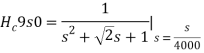
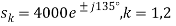
Q. Given  , that has a sampling frequency of 5Hz. Find the transfer function of the IIR digital filter.
Solution:
Step 1:

Step 2:
Applying partial fractions on H(s),

Step 3:
Step 4:
The bilinear transform is the result of a numerical integration of the analog transfer function into the digital domain. We can define the bilinear transform as:

Find the bilinear transformation which maps points z =2,1,0 onto the points w=1,0,i.
Ans. Let, 
And, 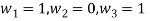
Since bilinear transformation preserves cross ratios,
Thus we have,

Use the bilinear transformation to convert the analog filtrt with system function
 into a digital IIR filter. Select T =0.1
Consider the following system function

Note that the following is the resonant frequency of the analog filter

Consider that the resonant frequency of analog filter must be mapped by selecting the value of parameter
T= 0,1
Use the following mapping for bilinear transformation

Write the system function H(z) of the resultant digital filter
Frequency warping
- The bilinear transformation method has the following important features: A stable analog filter gives a stable digital filter. t The maxima and minima of the amplitude response in the analog filter are preserved in the digital filter. As a consequence, – the pass band ripple, and – the minimum stop band attenuation of the analog filter is preserved in the digital filter frame.
- To determine the frequency response of a continuous-time filter, the transfer function Ha(s)Ha(s) is evaluated at s=jω which is on the jω axis. Likewise, to determine the frequency response of a discrete-time filter, the transfer function Hd(z) is evaluated at z=ejωT which is on the unit circle, |z|=1|z|=1.
- When the actual frequency of ω is input to the discrete-time filter designed by use of the bilinear transform, it is desired to know at what frequency, ωa, for the continuous-time filter that this ω is mapped to.


- This shows that every point on the unit circle in the discrete-time filter z-plane, z= ejωT is mapped to a point on the jω axis on the continuous-time filter s-plane, s=jω. That is, the discrete-time to continuous-time frequency mapping of the bilinear transform is
ωa=(2/T) tan(ωt/2)
And the inverse mapping is
ω=(2/T) arc tan(ωaT/2)
- The discrete-time filter behaves at frequency the same way that the continuous-time filter behaves at frequency (2/T)tan(ωT/2). Specifically, the gain and phase shift that the discrete-time filter has at frequency ω is the same gain and phase shift that the continuous-time filter has at frequency (2/T)tan(ωT/2). This means that every feature, every "bump" that is visible in the frequency response of the continuous-time filter is also visible in the discrete-time filter, but at a different frequency. For low frequencies (that is, when ω≪2/T or ωa≪2/T),ω≈ωa.
One can see that the entire continuous frequency range
−∞<ωa<+∞
Is mapped onto the fundamental frequency interval
−πT<ω<+πTω=±π/T.ωa=±∞
One can also see that there is a nonlinear relationship between ωa and ω This effect of the bilinear transform is called frequency warping.

Fig: Frequency Wrapping
Q. Design a discrete time lowpass filter to satisfy the following amplitude specifications: 

Assume 
The pre-warped critical frequency are


Since both the passband and stopband are required to be monotonic, a Butterworth approximation will be used


From the Butterworth design tables we can immediately write

Now find H (z) by first noting that


Using the pole/ zero mapping formula
We can now write
Find  by setting


Finally after multiplying out the numerator and denominator we obtain

Compare:
Sr No. | Impulse Invariance | Bilinear Transformation |
1 | In this method IIR filters are designed having a unit sample response h (n) that is sampled version of the impulse response of the analog filter. | This method of IIR filter design is based on the trapezoidal formula for numerical integration. |
2 | The bilinear transformation is a conformal mapping that transforms the j  | The bilinear transformation is a conformal mapping tjat transforms the  |
3 | For design of LPF, HPF and almost all types of bandpass and band stop filters this method is used. | For designing of LPF, HPF and almost all types of bandpass and band stop filters this method is used. |
4 | Frequency relationship is non –linear. Frequency warping or frequency compression is due to non – linearity. | Frequency relationship is non linear. Frequency warping or frequency compression is due to non – linearity. |
5 | All poles are mapped from s plane to the z plane by the relationship  | All poles and zeros are mapped. |
At the expense of steepness in transition medium from pass band to stop band this Butterworth filter will provide a flat response in the output signal. So, it is also referred as a maximally flat magnitude filter. The rate of falloff response of the filter is determined by the number of poles taken in the circuit. The pole number will depend on the number of the reactive elements in the circuit that is the number of inductors or capacitors used in the circuits.
The amplitude response of nth order Butterworth filter is given as follows:
Vout / Vin = 1 / √{1 + (f / fc)2n}
Where ‘n’ is the number of poles in the circuit. As the value of the ‘n’ increases the flatness of the filter response also increases.
'f' = operating frequency of the circuit and 'fc' = centre frequency or cut off frequency of the circuit.
These filters have pre-determined considerations whose applications are mainly at active RC circuits at higher frequencies. Even though it does not provide the sharp cut-off response it is often considered as the all-round filter which is used in many applications.
First Order Low Pass Butterworth Filter
The below circuit shows the low pass Butterworth filter:
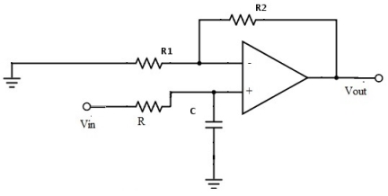
Fig: First order LP Butterworth Filter
The required pass band gain of the Butterworth filter will mainly depends on the resistor values of ‘R1’ and ‘Rf’ and the cut off frequency of the filter will depend on R and C elements in the above circuit.
The gain of the filter is given as Amax = 1 + (R1 / Rf)
The impedance of the capacitor ‘C’ is given by the -jXC and the voltage across the capacitor is given as,
Vc = - jXC / (R - jXC) * Vin
Where XC = 1 / (2πfc), capacitive Reactance.
The transfer function of the filter in polar form is given as
H(jω) = |Vout/Vin| ∟ø
Where gain of the filter Vout / Vin = Amax / √{1 + (f/fH)²}
And phase angle Ø = - tan-1 ( f/fH )
At lower frequencies means when the operating frequency is lower than the cut-off frequency, the pass band gain is equal to maximum gain.
Vout / Vin = Amax i.e. constant.
At higher frequencies means when the operating frequency is higher than the cut-off frequency, then the gain is less than the maximum gain.
Vout / Vin < Amax
When operating frequency is equal to the cut-off frequency the transfer function is equal to Amax /√2. The rate of decrease in the gain is 20dB/decade or 6dB/octave and can be represented in the response slope as -20dB/decade.
Second Order Low Pass Butterworth Filter
An additional RC network connected to the first order Butterworth filter gives us a second order low pass filter. This second order low pass filter has an advantage that the gain rolls-off very fast after the cut-off frequency, in the stop band.

Fig: Second Order LP Butterworth Filter
In this second order filter, the cut-off frequency value depends on the resistor and capacitor values of two RC sections. The cut-off frequency is calculated using the below formula.
fc = 1 / (2π√R2C2)
The gain rolls off at a rate of 40dB/decade and this response is shown in slope -40dB/decade. The transfer function of the filter can be given as:
Vout / Vin = Amax / √{1 + (f/fc)4}
The standard form of transfer function of the second order filter is given as
Vout / Vin = Amax /s2 + 2εωns + ωn2
Where ωn = natural frequency of oscillations = 1/R2C2
ε = Damping factor = (3 - Amax ) / 2
For second order Butterworth filter, the middle term required is sqrt(2) = 1.414, from the normalized Butterworth polynomial is
3 - Amax = √2 = 1.414
In order to have secured output filter response, it is necessary that the gain Amax is 1.586.
Higher order Butterworth filters are obtained by cascading first and second order Butterworth filters.
n (order) | Normalized Denominator polynomials in factored form |
1 |  |
2 |  |
3 |  |
The transfer function of the nth order Butterworth filter is given as follows:
H(jω) = 1/√{1 + ε² (ω/ωc)2n}
Where n is the order of the filter
ω is the radian frequency and it is equal to 2πf
And ε is the maximum pass band gain, Amax
Numerical:
Let us consider the Butterworth low pass filter with cut-off frequency 15.9 kHz and with the pass band gain 1.5 and capacitor C = 0.001µF.
fc = 1/2πRC
15.9 * 10³ = 1 / {2πR1 * 0.001 * 10-6}
R = 10kΩ
Amax = 1.5 and assume R1 as 10 kΩ
Amax = 1 + {Rf / R1}
Rf = 5 kΩ

Ideal Frequency Response of the Butterworth Filter
The flatness of the output response increases as the order of the filter increases. The gain and normalized response of the Butterworth filter for different orders are given below:

Fig: Frequency Response of Butterworth Filter
Example. A Butterworth Amplitude Response design
Let, 

Solving for N gives
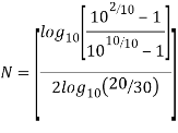

Matching at 

The normal  from the table is
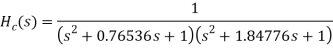
Frequency seal  impliea that we let
Finally, the frequency scaled system function is

A Chebyshev design achieves a more rapid roll-off rate near the cut-off frequency than the Butterworth by allowing ripple in the passband (type I) or stopband (type II). Monotonicity of the stopband or passband is still maintained respectively.

Fig: Chebyshev Filter Type I and II
Chebyshev Type I
The magnitude response is given by

Where,
 Nth order Chebyshev polynomial
And  specifies the passband ripple
The Chebyshev polynomials are of the form\
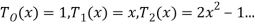
With recurrence formula

An alternate form for  which will be useful in both analysis and design is

Design a Chebyshev type I lowpass filter to satisfy the following amplitude specification 
Using the design formula for N
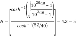
From the 2dB ripple table (9-20)

Elliptic Design
Allows both passband and stopband ripple to obtain a narrow transition band. The elliptic (Cauer) filter is optimum in the sense that no other filter of the same order can provide a narrower transition band.
The squared magnitude response is given by


Define the transition region ratio as

The normalized lowpass system function can be written in factored form as

Note:  contains conjugate pairs of zeros on the j
 axis which give the stopband nulls.
The filter coefficients  if N is odd.
Design an elliptic lowpass filter to satisfy the following amplitude specifications, 
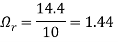
From the 1dB ripple, 40Db stopband attenuation table wew find that N meets or exceeds the
  = 1.2187, so we can scale
 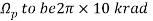 and then the desired stopband attenuation will actually be achieved at
  .
.
T6he normalized H (z)  is
is
H(s)=(0.046998s4+0.22007s2+0.22985)/(s5+0.92339s4+1.84712s3+1.12923s2+0.78813s
To complete the design scale H (s) by letting 
Example. Design from a Rational H (s)
Let, 
Inverse Laplace transforming yields

Sampling  seconds and gain scaling we obtain

Which implies that

Setting  requires that
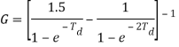
Q. Design a Chebyshev type 1 low pass filter to satisfy the following amplitude specifications: 
Using the design formula for N
N = [2.08]=3
Note: 
The normalized system function is

With poles at

To frequency scale  let
let

So in the z domain

Note that when the design originates from discrete time specifications the poles of H (z) are independent of  .
.
Direct form I
The difference equation


Specifies the Direct-Form I (DF-I) implementation of a digital filter. The DF-I signal flow graph for the second-order case is shown in Fig.

Figure: Direct-Form-I implementation of a 2nd-order digital filter.
Direct form II
The signal flow graph for the Direct-Form-II (DF-II) realization of the second-order IIR filter section is shown in Fig.

Figure: Direct-Form-II implementation of a 2nd-order digital filter.
The difference equation for the second-order DF-II structure can be written as


Which can be interpreted as a two-pole filter followed in series by a two-zero filter.

Fig. Transposed-Direct-Form-I

Fig. Transposed-Direct-Form-II implementation of a second-order IIR digital filter
The filter section can be seen to be an FIR filter and can be realized as shown below
W[n] = p0x[n] + p1x[n-1] + p2x[n-2] +p3x[n-3]

The time-domain representation of H2(z) is given by
Y[n] = w[n] –d1y[n-1] –d2y[n-2] – d3y[n-3]

A cascade of the two structures realizing and leads to the realization of shown below and is known as the direct form I structure

Fig: Cascade form
Direct form II and cascade form realizations of


Fig: Direct form II

Fig: Cascade form
The parallel form is obtained from

Based on the above equation, we need the current input sample and M−1 previous samples of the input to produce an output point. For M=5, we can simply obtain the following diagram from Equation 1.

On the other hand, for a linear-phase FIR filter, we observe the following symmetry in coefficients of the difference equation
The structure obtained from the above equation is shown in Figure 2. While Figure 1 requires five multipliers, employing the symmetry of a linear-phase FIR filter, we can implement the filter using only three multipliers. This example shows that for an odd M, the symmetry property reduces the number of multipliers of an (M−1)th-order FIR filter from M to M+1/2.

Example. A partial fraction expansion of
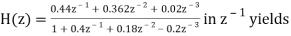
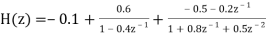
The corresponding parallel form I realization is shown below

Lattice IIR Structure
Consider a system with finite poles and all its zeros at z = 0 whose transfer function is of the form
H(z) = 
Where AN(z) = 1 +  is an Nth degree polynomial in z. This system has N finite poles and N zeros at z = 0.
Lattice IIR Direct form II Structure
A Direct Form II system with N finite poles and N zeros at z = 0.
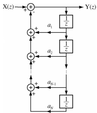
Fig. Lattice IIR Structure
Comparison of Direct Form II structures for FIR and IIR systems.
If, in the FIR system, we exchange the roles of X (z) and Y (z),change allb's to -a's (with b0 = 1) and let N = M - 1, we get theIIR system.

Modify the FIR lattice structure as illustrated below. Reverse the arrows on all the "f" signals. Reverse the lattice and apply x [n] to the previous output and take y [n] from the previous input.
Also reverse the signs of the signals arriving from the bottom. This is now a recursive or feedback structure which can implement an IIR filter.

Fig. Lattice-Ladder IIR Structure
Take the case N = 1

z transforming
Y(z) + K1z-1Y(z) = X(z) H1(z) = 
Single pole at z = - K1 and a zero at z = 0.

Fig. Lattice-Ladder IIR Structure
Also, for the N = 1 case
g1[n] = K1y[n] + y[n – 1]
G1(z) = K1Y(z) + z-1Y(z) G1(z)/Y(z) = K1 + z-1 = K1 
G1(z)/Y(z) is the transfer function of a system with a single zero at
z = -1/K1 and a pole at zero.

Fig. Lattice-Ladder IIR Structure
For the N = 2 case, it can be shown that
H2(z) = Y(z)/X(z) = 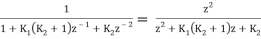
And
G2(z)/Y(z) = K2 + K1(K2 + 1)z-1 + z-2 = K2 
Notice that the coefficients for the FIR and IIR systems occur in reverse order as before.
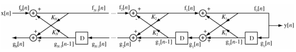
Fig. Lattice-Ladder IIR Structure
For any m,
Hm(z) = Y(z)/X(z) = 1/Am(z) and Gm(z)/Y(z) = Bm (z) = z-mAm(1/z)
And the previous relations for FIR lattices still hold.
A0(z) = B0(z) = 1, Am(z) = Am-1(z) + Kmz-1Bm-1(z)
Bm(z) = z-m Am(1/z), Km αm[m]
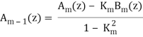

Fig. Lattice-Ladder IIR Structure
If we want to add finite zeros to Hm(z) we can add a ladder network to the lattice. Then the transfer function will be of the form.

y[n] = 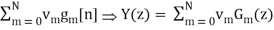

Lattice-Ladder Example
Synthesize the transfer function
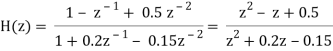
Using a lattice-ladder network.
A2(z) = 1+ 0.2z-1 – 0.15 z-2
K2 = -0.15 and B2(z) = -0.15 + 0.2z-1 + z-2
Γ2(z) = 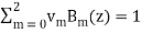 - z-1 + 0.5z-2 v2 = 0.5
Γ1(z) = Γ2(z) – v2B2(z) = 1 – z-1 + 0.5z-2 – 0.5 (- 0.15 + 0.2z-1 + z-2)
Γ1(z) = 1,075 – 1.1z-1 v1 = - 1.1
Γ0(z) = Γ1(z) – v1B1(z)
Lattice-Ladder Example
Using Am-1(z) = 
A1(z) = 
A1(z) = 
K1 = 0.23529 and B1(z) = 0.23529 + z-1
Γ0(z) = 1.075 – 1.1z-1 – (-1.1)(0.23529 + z-1) = 1.3382 v0 = 1.3382
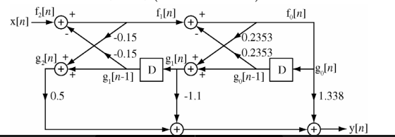
References:
1. Digital signal processing- A practical approach Second Edition, 2002.E. C. Ifeachar, B. W. Jarvis Pearson Education
2. Sanjit K. Mitra, ‘Digital Signal Processing – A Computer based approach’
3. S. Salivahanan, A Vallavaraj, C. Gnanapriya, ‘Digital Signal Processing’, 2nd Edition McGraw Hill.
4. A. Nagoor Kani, ‘Digital Signal Processing’, 2nd Edition McGraw Hill.
5. P. Ramesh Babu, ‘Digital Signal Processing’ Scitech


