Unit - 5
Design of Sinusoidal Oscillators, Function Generator and Filters
Wein Bridge Oscillators
Wien bridge oscillator is an audio frequency sine wave oscillator of high stability and simplicity. The feedback signal in this circuit is connected to the non-inverting input terminal so that the op-amp is working as a non-inverting amplifier.
The feedback network does not provide any phase shift. The circuit can be viewed as a Wien bridge with a series combination of R1 and C1 in one arm and parallel combination of R2 and C2 in the adjoining arm. Resistors R3 and R4 are connected in the remaining two arms.
The condition of zero phase shift around the circuit is achieved by balancing the bridge. The series and parallel combination of RC network form a lead-lag circuit.
At high frequencies, the reactance of capacitor C1 and C2 approaches zero. This causes C1 and C2 appears short. Here, capacitor C2 shorts the resistor R2. Hence, the output voltage Vo will be zero since output is taken across R2 and C2 combination. So, at high frequencies, circuit acts as a 'lag circuit'.
At low frequencies, both capacitors act as open because capacitor offers very high reactance. Again, output voltage will be zero because the input signal is dropped across the R1 and C1 combination. Here, the circuit acts like a 'lead circuit'.
But at one particular frequency between the two extremes, the output voltage reaches to the maximum value. At this frequency only, resistance value becomes equal to capacitive reactance and gives maximum output. Hence, this frequency is known as oscillating frequency (f).
Consider the feedback circuit, on applying voltage divider rule
Vf(s) = Vo(s) x Zp(s)/ Zp(s) + Zs(s)
Zs(s) = R1 + 1/sC1 and Zp(s) = R2|| 1/sC2
Let R1=R2=R and C1=C2=C . On solving
β = Vf(s)/ Vo(s) = RsC /(RsC) 2 + 3RsC + 1 ---------------------------(1)
Since the op-amp is operated in the non-inverting configuration the voltage gain
Av = Vo(s)/ Vf(s) = 1 + R3/R4 -------------------(2)
Applying the condition for sustained oscillations, = Av β =1
RsC /(RsC) 2 + 3RsC + 1. 1 + R3/R4
S=jw
(1 + R3/R4) ( jwRC/ - R2 C2 w2 + 3 jwRC + 1) =1
Jw RC (1 + R3/R4)= (- R2 C2 w2 + 3 jwRC + 1)
Jw[(1 + R3/R4)RC – 3RC] = 1- R2 C2 w2
To obtain the frequency of oscillation equate the real part to zero
1-R2 C2 w2 = 0
w = 1/RC
f = 1/ 2 π RC
To obtain the condition for gain at the frequency of oscillation equate the imaginary part to zero.
Jw[(1 + R3/R4)RC – 3RC] = 0
Jw[(1 + R3/R4)RC= jw3RC
[(1 + R3/R4) =3
R3/R4 =2
Therefore R3 = 2 R4 is the required condition.
Phase Shift oscillator
In an RC Oscillator circuit, the input is shifted 180o through the feedback circuit returning the signal out-of-phase and 180o again through an inverting amplifier stage to produces the required positive feedback.
This then gives us “180o + 180o = 360o” of phase shift which is effectively the same as 0o, thereby giving us the required positive feedback.
In other words, the total phase shift of the feedback loop should be “0” or any multiple of 360o to obtain the same effect.
The circuit on the left shows a single resistor-capacitor network whose output voltage “leads” the input voltage by some angle less than 90o.
In a pure or ideal single-pole RC network. It would produce a maximum phase shift of exactly 90o, and because 180o of phase shift is required for oscillation, at least two single-poles networks must be used within an RC oscillator design.
However, in reality it is difficult to obtain exactly 90o of phase shift for each RC stage so we must therefore use more RC stages cascaded together to obtain the required value at the oscillation frequency.
The amount of actual phase shift in the circuit depends upon the values of the resistor (R) and the capacitor (C), at the chosen frequency of oscillations with the phase angle ( φ ) being given as:
Xc = 1/2π fc R=R
Z = [ R 2 + Xc 2 ] ½
Ø = tan -1 Xc /R
Hartley Oscillator
It is most popular oscillator and is commonly used in radio receivers. It consists of 2 coil L1 and L2 wound over the same core. Thus, mutual inductance exists between terms. A capacitor C1 is connected to from L-C circuit. Rb provides the necessary biasing. The capacitor C block DC component.
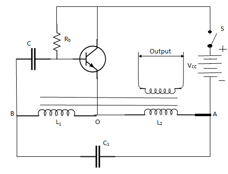
Fig. Hartley Oscillator
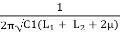
The frequency of oscillation is determined by L1,L2, and C1.
When Switch C1 discharge through L1 and L2, setting up oscillation of frequency f, given by
F =  =
= 
The oscillation between 0 and B drives the transistor and output appears at the collector which supplies the losses.
It may be noted that L1 and L2 are magnetically linked with each other so that points B and A are 180° out of phase. A further shift of 180° is produced by transistor. Thus, it ensures proper positive feedback and results in undamped oscillations.
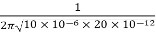
Que) In a transistor Hartley oscillator if L1 = 0.1 m H, L2 = 10  H and mutual inductance between the two coil M = 20
  H, calculate the value of capacitor C1 of oscillatory circuit to obtain frequency of 4110 kHz
Sol-
L1 = 100  H
H
L2 = 10  H
H
M = 20  H
H
Total inductance, L = L1 + L2 + 2M
= 100 + 10 + 2 × 20
= 150  H
H
F = 
4110× 103 = 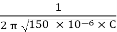
 × 150 × 10-6 × C =
C = 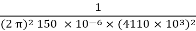 = 10pf
Colpitt’s Oscillator
It is similar to Hartley. The only difference is that in case of Colpitt’s oscillator, coupling is capacitive instead of being inductive.
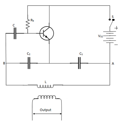
Fig. Colpitts Oscillator
In this the tank circuit consist of inductor L in parallel with 2 capacitors C1 and C2 which are in series. The resistor Rb provider the necessary biasing and capacitor C blocks the d.c. Component. The frequency of oscillations is given by
F = 
Where CT – Total Capacitance 
When switch S is closed, capacitor C1 and C2 are charged. These capacitors discharge through L, setting up of oscillation of frequency F
The oscillation across C2 is applied to transistor which gets amplified. This amplified output is fed to the oscillatory circuit in order to supply the losses. In this way it ensures undamped oscillations.
A phase difference of 180° is created between A and B and a further phase shift of 180° is produced by transistor action.
Que) Find the operating frequency of a transistor Colpitt’s oscillator if C1 = 30 pf, C2 = 60Þf and L = 10  H
H
Sol- Total capacitance, CT =  =
=  = 20 pf = 20× 10-12 F
Inductance, L = 10 H = 10× 10-6 H
F = 
=  = 11.25 MH
Crystal Oscillator can be designed by connecting the crystal into the circuit such that it offers low impedance when operated in series-resonant mode and high impedance when operated in anti-resonant or parallel resonant mode as shown below in figure a and b respectively.
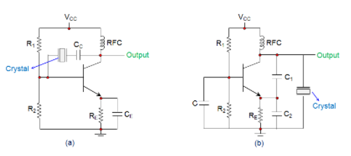
Fig (a) Series Resonance Fig (b) Parallel Resonance
In the circuits shown, the resistor R1 and R2 form the voltage divider network while the emitter resistor RE stabilizes the circuit. Further, CE (Figure a) acts as an AC bypass capacitor while the coupling capacitor CC (Figure a) is used to block DC signal propagation between the collector and the base terminals. Next, the capacitors C1 and C2 form the capacitive voltage divider network in the case of Figure b.
In addition, there is also a Radio Frequency Coil (RFC) in the circuits (both in Figure a and b) which offers dual advantage as it provides even the DC bias as well as frees the circuit-output from being affected by the AC signal on the power lines.
On supplying the power to the oscillator, the amplitude of the oscillations in the circuit increases until a point is reached wherein the nonlinearities in the amplifier reduce the loop gain to unity. Next, on reaching the steady-state, the crystal in the feedback loop highly influences the frequency of the operating circuit.
Further, here, the frequency will self-adjust so as to facilitate the crystal to present a reactance to the circuit such that the Barkhausen phase requirement is fulfilled.
In general, the frequency of the crystal oscillators will be fixed to be the crystal’s fundamental or characteristic frequency which will be decided by the physical size and shape of the crystal.
However, if the crystal is non-parallel or of non-uniform thickness, then it might resonate at multiple frequencies, resulting in harmonics. Further, the crystal oscillators can be tuned to either even or odd harmonic of the fundamental frequency, which are called Harmonic and Overtone Oscillators, respectively.
Key takeaway
Crystal Oscillator can be designed by connecting the crystal into the circuit such that it offers low impedance when operated in series-resonant mode and high impedance when operated in anti-resonant or parallel resonant mode.
First Order Active Low Pass Filter
It is a simplistic filter that is composed of only one reactive component Capacitor accompanying with an active component Op-Amp. A resistor is utilized with the capacitor or inductor to form RC or RL low pass filter respectively. In a passive circuit, the output signal amplitude is smaller than the input signal amplitude. To surmount this problem, active circuit designs were introduced. When a passive low pass filter is connected to an Op-Amp either in inverting or non-inverting condition, it gives an active low pass filter design. The connection of a simple RC circuit with a single Op-Amp is shown in the image below.
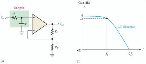
Fig. First Order Active Low Pass Filter with the frequency response
This RC circuit assists in providing a low-frequency signal to the input of the amplifier. The amplifier operates as a unity gain output buffer circuit. This circuit has added input impedance value. The Op-Amp of the circuit has a very low output impedance value, which helps in providing high stability to the filter.
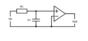
Fig. Active Low Pass Filter Circuit
First Order Active Low Pass Filter with Amplification
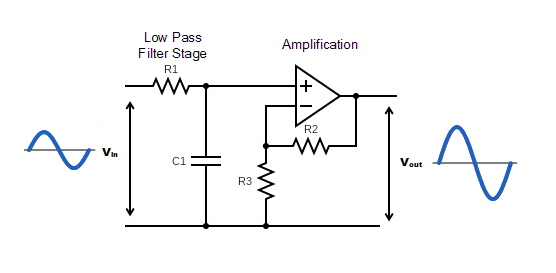
Fig. Active Low Pass Filter with Amplification
In a non-inverting amplifier circuit configuration, the measurement of the voltage gain for the filter is given as a ratio of the feedback resistor ( R2 ) divided by its corresponding input resistor ( R3 ) value.

First Order Low Pass Filter Voltage Gain
The frequency components are used to obtain the voltage gain of the filter.
Voltage gain 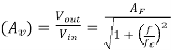
Where,
Vin is the input voltage
Vout is the output voltage
Af is the passband gain of the filter (1+R2/R1)
f is the frequency of the input signal in Hertz
fc is the cutoff frequency in Hertz
When the frequency is increased, then the gain is decreased by 20 dB. The operation of an active low pass filter can be checked from the above equation of frequency gain. Let f be the operating frequency and fc be the cutoff frequency.
At low frequency

When operating frequency is equal to cut off frequency

And at high frequency

From the above equations, it is seen that at low frequencies the gain of the circuit is equal to the maximum value of gain.
Whereas at high frequencies condition, the gain of the circuit is very much lesser than the maximum gain Af.
When the operating frequency is equal to cut off frequency, the gain is equal to 0.707 Af.
In these filter circuits, the quantitative value (magnitude) of the passband gain is expressed in decibels or dB which is a function of the voltage gain.
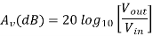
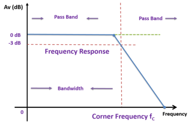
Fig. Frequency Response Curve
Design:
Example-1
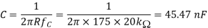
Design a non-inverting active low pass filter circuit that has a gain of ten at low frequencies, a high-frequency cut-off or corner frequency of 175Hz and an input impedance of 20KΩ.
The voltage gain of the non-inverting amplifier is given as
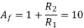
Now assume the value of R1 to be 1KΩ and calculate the value R2 from the above equation.

Hence for a voltage gain of 10, values of R1 and R2 are 1KΩ and 9KΩ respectively. Gain in dB is given as 20LogA = 20Log10 = 20dB
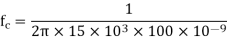
Now we are given with the cut-off frequency value as 175Hz and input impedance value as 20KΩ. By substituting these values in the equation and value of C can be calculated as follows.

Active Low Pass Filter Circuit
A typical circuit for an active low pass filter is given below:
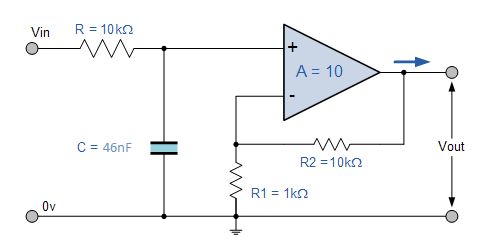
Fig. Circuit design
Active Low Pass Filter Frequency Response Curve
The frequency response curve for an active low pass filter is given below:
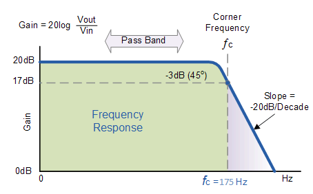
Fig. Frequency Response of the problem
Non-Inverting Amplifier Filter
A simple non-inverting amplifier filter is given below:
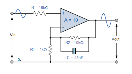
Fig. Non-inverting circuit for the problem
Inverting Amplifier Filter
An equivalent inverting amplifier filter is given below:
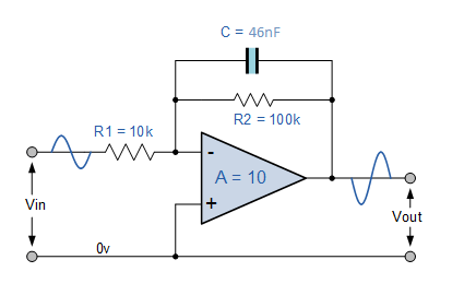
Fig. Equivalent inverting circuit for the problem
Second Order Active Low Pass Filter
Second-Order Filters are also attributed to as VCVS filters since Op-Amp used here is Voltage Controlled Voltage Source Amplifier. This is another important type of active filter used in applications. The frequency response of the second-order low pass filter is indistinguishable to that of the first-order type besides that the stopband roll-off will be twice the first-order filters at 40dB/decade. Consequently, the design steps wanted of the second-order active low pass filter are identical. A simple method to get a second-order filter is to cascade two first-order filters.
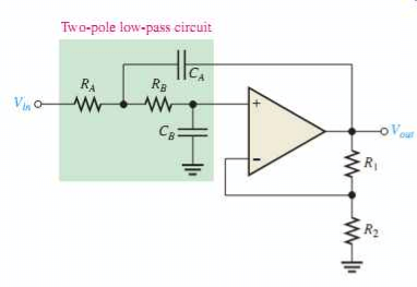
Fig. Second-Order Active Low Pass Filter
Second Order Active Low Pass Filter Design and Example
Example-2
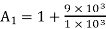
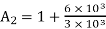
Assume Rs1 = Rs2 = 15KΩ and capacitor C1 = C2 = 100nF. The gain resistors are R1=1KΩ, R2= 9KΩ, R3 = 6KΩ, and R4 =3KΩ. Design a second-order active low pass filter with these specifications.
The cut-off frequency is given as

(1)

The gain of first stage amplifier is


The gain of second stage amplifier is


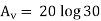
Total Gain of the filter


The total gain in dB
(2) 
(3) 
The gain at cut-off frequency is
(4) Gain at 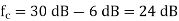
Design and frequency scaling of First order and second order Active HP
The basic operation of an Active High Pass Filter (HPF) is the same as for its equivalent RC passive high pass filter circuit, except this time the circuit has an operational amplifier or included within its design providing amplification and gain control.
First Order High Pass Filter
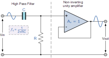
Fig. First Order HPF
Frequency response curve of a typical Operational Amplifier
Fig. Frequency response curve of a typical Operational Amplifier
Then the performance of a “high pass filter” at high frequencies is limited by this unity gain crossover frequency which determines the overall bandwidth of the open-loop amplifier.
Example-3
Consider cut-off frequency value as 10 KHz, pass band gain Amax as 1.5 and capacitor value as 0.02 µF.
The equation of the cut-off frequency is fC = 1 / (2πRC)
By re-arranging this equation,
We have R = 1 / (2πfC)
R = 1/ (2π * 10000 * 0.02 * 10-6) = 795.77 Ω
The pass band gain of the filter is Amax = 1 + (R3/R2) = 1.5
R3 = 0.5 R2
If we consider the R2 value as 10KΩ, then R3 = 5 kΩ
We can calculate the gain of the filter as follows:
Voltage Gain for High Pass filter:
| Vout / Vin | = Amax * (f/fc) /√ [1 + (f/fc)²]
Av(dB) = 20 log10 (Vout/Vin)
Second Order High Pass Filter Circuit
The designing procedure for the second order active filter is same as that of the first order filter because the only variation is in the roll-off. If the roll-off of the first order active high pass filter is 20dB/decade, then roll-off of the second order filter is 40 dB/ decade. It means the twice of the value of the first order filter. The circuit of second order filter is shown below:
Fig. Second Order HPF
The gain of the filter is 1+ R1/R2 and the equation of the cut-off frequency is fc = 1/ 2π√R3R4C1C2
Second Order High Pass Filter Example
Design a filter with cut-off frequency 4 KHz and the delay rate in the stop band is 40dB/decade. As the delay rate in the stop band is 40dB/decade we can clearly say that the filter is second order filter.
Let us consider the capacitor values as C1= C2 = C = 0.02µF
The equation of the cut-off frequency is fc = 1/ 2πRC Hz
By re-arranging this equation we have R = 1/ 2πfC
By substituting the values of cut-off frequency as 4 KHz and capacitor as 0.02µF
R = 1.989 KΩ = 2KΩ.
Let the gain of the filter is 1+ R1/R2 = 2
R1 / R2 = 1
R1 = R2
Therefore, we can take R1 = R2 = 10 KΩ
Thus, the obtained filter is shown as below:
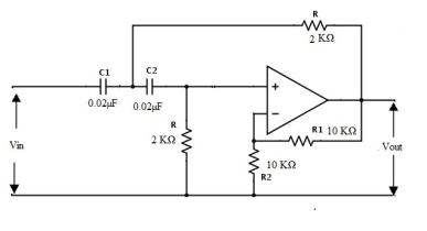
Fig. HPF Designed circuit
Design and frequency scaling of First order and second order Active BP
A Band Pass Filter is a circuit which allows only particular band of frequencies to pass through it. This Pass band is mainly between the cut-off frequencies and they are fL and fH, where fL is the lower cut-off frequency and fH is higher cut-off frequency.
The center frequency is denoted by ‘fC’ and it is also called as resonant frequency or peak frequency.
Combination of low pass and high pass responses gives us band pass response as shown below:
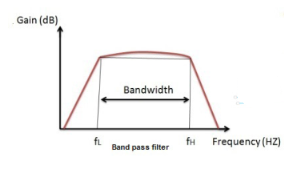
Fig. BPF response
Active Band pass filter:
Depending on the quality factor the band pass filter is classified into Wide band pass filter and Narrow band pass filter. The quality factor is also referred as ‘figure of merit’. By cascading High Pass Filter and Low Pass Filter with an amplifying component we obtain band pass filter.
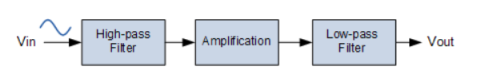
Fig. BPF block diagram
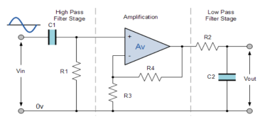
Fig. BPF
Fig. Bandwidth of BPF
Example-4
Consider the infinity gain multiple feedback active filter circuit for which the resonating frequency is 1.5 kHz, maximum Voltage gain is 15 and quality factor is 7. Then component values are calculated as follows:
For Resistors
R1 =Q/ 2πfc CAmax
R2 = Q/ πfc C
And R3 = Q/ 2πfc C(2Q2 - Amax)
Choosing capacitor C1 =C2 =C = 0.02µF
Q= fc / Bandwidth = 0.5 √(R2/ R1) = 7
Applying values to R1, R2, R3 we get R1 = 2.47kΩ , R2 = 74.27 kΩ , R3 = 447.4 kΩ.
We consider that the changed resistor value as R3´ and the changed cut-off frequency value fc´=2 KHz then we can equate for the new resistor value as follows:
R3´ = R3 (fc/fc´)2 = 447.4(1.5/2)2 = 251.66 Ω
Therefore, simply by taking the required frequency we can calculate the new resistor value.
Example 5:
An active band pass filter that has a voltage gain Av of one (1) and a resonant frequency, ƒr of 1kHz is constructed using an infinite gain multiple feedback filter circuit. Calculate the values of the components required to implement the circuit.
Firstly, we can determine the values of the two resistors, R1 and R2 required for the active filter using the gain of the circuit to find Q as follows.
Av = 1 = -2Q2
QBP = √(1/2) =0.7071
Q = 0.7071 = 0.5 √(R1/R2)
Or R1/R2 =2
Then we can see that a value of Q = 0.7071 gives a relationship of resistor, R2 being twice the value of resistor R1. Then we can choose any suitable value of resistances to give the required ratio of two. Then resistor R1 = 10kΩ and R2 = 20kΩ.
The center or resonant frequency is given as 1kHz. Using the new resistor values obtained, we can determine the value of the capacitors required assuming that C = C1 = C2.
F1 = 1000 Hz = 
C =  =
=  =11.2nF
The closest standard value is 10nF.
Wide and narrow band BR Butter worth filters and notch filter
The frequency response of the Butterworth Filter approximation function is also often referred to as “maximally flat” (no ripples) response because the pass band is designed to have a frequency response which is as flat as mathematically possible from 0Hz (DC) until the cut-off frequency at -3dB with no ripples. Higher frequencies beyond the cut-off point rolls-off down to zero in the stop band at 20dB/decade or 6dB/octave. This is because it has a “quality factor”, “Q” of just 0.707.
However, one main disadvantage of the Butterworth filter is that it achieves this pass band flatness at the expense of a wide transition band as the filter changes from the pass band to the stop band. It also has poor phase characteristics as well. The ideal frequency response, referred to as a “brick wall” filter, and the standard Butterworth approximations, for different filter orders are given below.
Ideal Frequency Response for a Butterworth Filter
Fig. Frequency response for butter worth filter
Note that the higher the Butterworth filter order, the higher the number of cascaded stages there are within the filter design, and the closer the filter becomes to the ideal “brick wall” response.
In practice however, Butterworth’s ideal frequency response is unattainable as it produces excessive passband ripple.
Where the generalized equation representing a “nth” Order Butterworth filter, the frequency response is given as:
H(jw) = 1/ √(1+ €2(w/wp)2n)
Where: n represents the filter order, Omega ω is equal to 2πƒ and Epsilon ε is the maximum pass band gain, (Amax). However, if you now wish to define Amax at a different voltage gain value, for example 1dB, or 1.1220 (1dB = 20*logAmax) then the new value of epsilon, ε is found by:
H1 = H0 (1 + €2)1/2 |
|
Transpose the equation to give:
H0/H1 =1.1220 =(1 + €2)1/2 gives € = 0.5088
The Frequency Response of a filter can be defined mathematically by its Transfer Function with the standard Voltage Transfer Function H(jω) written as:
 |
|
Note: ( jω ) can also be written as ( s ) to denote the S-domain. and the resultant transfer function for a second-order low pass filter is given as:
 = (S2 + S+ 1)-1/2
Example-6:
Find the order of an active low pass Butterworth filter whose specifications are given as: Amax = 0.5dB at a pass band frequency (ωp) of 200 radian/sec (31.8Hz), and Amin = -20dB at a stop band frequency (ωs) of 800 radian/sec. Also design a suitable Butterworth filter circuit to match these requirements.
Firstly, the maximum pass band gain Amax = 0.5dB which is equal to a gain of 1.0593, remember that: 0.5dB = 20*log(A) at a frequency (ωp) of 200 rads/s, so the value of epsilon ε is found by:
1.0593 = =(1 + €2)1/2
€ = 0.3495
Secondly, the minimum stop band gain Amin = -20dB which is equal to a gain of 10 (-20dB = 20*log(A)) at a stop band frequency (ωs) of 800 rads/s or 127.3Hz.
Substituting the values into the general equation for a Butterworth filters frequency response gives us the following:
H(jw) = 1/ √(1+ €2(w/wp)2n)
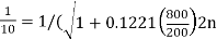
(10)2 = 1 + 0.1221 x 42n
On solving this we get n = 2.42
Since n must always be an integer ( whole number ) then the next highest value to 2.42 is n = 3, therefore a “a third-order filter is required” and to produce a third-order Butterworth filter, a second-order filter stage cascaded together with a first-order filter stage is required.
From the normalised low pass Butterworth Polynomials table above, the coefficient for a third-order filter is given as (1+s)(1+s+s2) and this gives us a gain of 3-A = 1, or A = 2. As A = 1 + (Rf/R1), choosing a value for both the feedback resistor Rf and resistor R1 gives us values of 1kΩ and 1kΩ respectively as: ( 1kΩ/1kΩ ) + 1 = 2.
We know that the cut-off corner frequency, the -3dB point (ωo) can be found using the formula 1/CR, but we need to find ωo from the pass band frequency ωp then,
NOTCH FILTERS
Notch filters, also commonly referred to as band-stop or band-rejection filters, are designed to transmit most wavelengths with little intensity loss while attenuating light within a specific wavelength range (the stop band) to a very low level. They are essentially the inverse of band pass filters, which offer high in-band transmission and high out-of-band rejection so as to only transmit light within a small wavelength range.
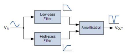
Fig. Notch Filter
Notch filters are useful in applications where one needs to block light from a laser. For instance, to obtain good signal-to-noise ratios in Raman spectroscopy experiments, it is critical that light from the pump laser be blocked. This is achieved by placing a notch filter in the detection channel of the setup. In addition to spectroscopy, notch filters are commonly used in laser-based fluorescence instrumentation and biomedical laser systems.
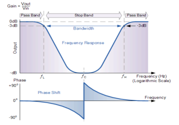
Fig. Band stop frequency response
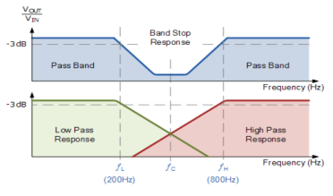
Fig. Band stop frequency characteristics
Example-7
Design a basic wide-band, RC band stop filter with a lower cut-off frequency of 200Hz and a higher cut-off frequency of 800Hz. Find the geometric center frequency, -3dB bandwidth and Q of the circuit.
F = 1/ 2πRC
The upper and lower cut-off frequency points for a band stop filter can be found using the same formula as that for both the low and high pass filters as shown.
Assuming a capacitor, C value for both filter sections of 0.1uF, the values of the two frequency determining resistors, RL and RH are calculated as follows.
Low Pass Filter Section
FL = 1/ 2πRLC = 200Hz and C =0.1 µF
RL = 1/ 2π x 200 x 0.1 10 -6 = 7958Ω or 8kΩ
High Pass Filter Section
FH = 1/ 2πRHC = 800Hz and C =0.1 µF
RH = 1/ 2π x 800 x 0.1 10 -6 = 1990Ω or 2kΩ
From this we can calculate the geometric center frequency, ƒC as:
Fc = √(fL x fH) = √(200x 800) = 400 Hz
fBW = fH - fL = 800 – 200 =600 Hz
Q = Fc/ fBW = 400/600 = 0.67 OR -3.5 dB
If we make the op-amps feedback resistor and its two input resistors the same values, say 10kΩ, then the inverting summing circuit will provide a mathematically correct sum of the two input signals with zero voltage gain.
Then the final circuit for our band stop (band-reject) filter example will be:
Band Stop Filter Design
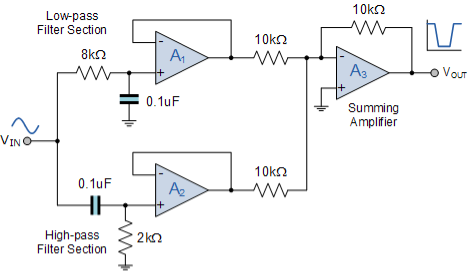
Fig. Band Stop Filter
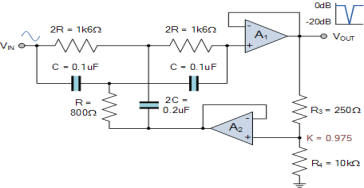
Example-8:
Design a two op-amp narrow-band, RC notch filter with a center notch frequency, ƒN of 1kHz and a -3dB bandwidth of 100 Hz. Use 0.1uF capacitors in your design and calculate the expected notch depth in decibels.
Data given: ƒN = 1000Hz, BW = 100Hz and C = 0.1uF.
1. Calculate value of R for the given capacitance of 0.1uF
R =  x 106
x 106
R = 795 Ω
2. Calculate value of Q
Q = FN/ fBW = 1000/100 =10
3. Calculate value of feedback fraction k
K = 1 – 1/4Q =1- 1/ 4x 10 = 0.975
4. Calculate the values of resistors R3 and R4
K = 0.975 = R4/(R3+R4)
Assuming R4 = 10kΩ then R3 is
R3 = R4 – 0.975 X R4
R3 =250Ω
5. Calculate expected notch depth in decibels, dB
1/Q =1/10 =0.1
fN(dB) = 20 log (0.1) = -20dB
Notch Filter Design
All pass filters
An all-pass filter is that which passes all frequency components of the input signal without attenuation but provides predictable phase shifts for different frequencies of the input signals. The all-pass filters are also called delay equalizers or phase correctors. An all-pass filter with the output lagging behind the input is illustrated in figure.
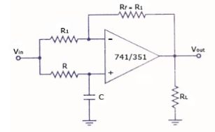
Fig. Circuit diagram
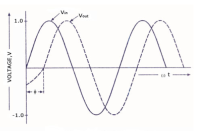
Fig. Input, output waveform
The output voltage vout of the filter circuit shown in fig. (a) can be obtained by using the superposition theorem
vout = -vin +[ -jXC/R-jXC]2vin
Substituting -jXC = [1/j2∏fc] in the above equation, we have
vout = vin [-1 +( 2/ j2∏Rfc)]
Or vout / vin = 1- j2∏Rfc/1+ j2∏Rfc
The Transfer function of All Pass Filter can be expressed as mentioned above. It can be synthesized to the following equation:
HAP = HLP - HBP + HHP = 1 - 2* HBP
The function of All Pass filter is
- To introduce phase shift or phase delay to the response of the circuit.
- Amplitude of the filter is unity for all the frequencies.
- Phase response is changing from 0 degree to 360 degree.
Key takeaways
- It can be used as a phase corrector.
- It is used to compensate the phase changes of voice signals that may have occurred over telephone wires during transmission.
- It is used in single side band suppressed carrier i.e. SSB-SC modulation based circuit designs.
References:
1. David A. Bell, ‘Op-amp & Linear ICs’, Oxford, 2013.
2. D. Roy Choudhary, Sheil B. Jani, ‘Linear Integrated Circuits’, II edition, New Age, 2003.
3. Ramakant A. Gayakward, ‘Op-amps and Linear Integrated Circuits’, IV edition, Pearson Education, 2003 / PHI. 2000.
4. N. C. Goyal and Khetan ‘A Monograph on Electronics Design Principals’, Khanna Publications
5. Sergio Franco, “Design with Operational Amplifiers and Analog Integrated Circuits”, McGraw Hill.


