UNIT 2
Rectifiers and Filters
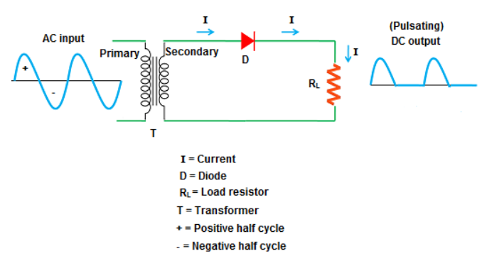
- It is the simplest form of the rectifier. Here, a single diode is used .
- It consists of an AC source, transformer (step-down), diode, and resistor (load).
- The diode is placed between the transformer and resistor (load).

Operation:
- It allows only half cycle and blocks the other half cycle.
- When it allows positive half cycles and blocks negative half cycles, it is called a positive half wave rectifier. The output DC current or DC signal produced by a positive half wave rectifier is a series of positive half cycles or positive sinusoidal pulses.
- When it allows electric current during the negative half-cycle of input AC signal and blocks electric current during the positive half-cycle of the input AC signal.
- A negative half wave rectifier produces a series of negative sinusoidal pulses.
- For an ideal diode, the positive half cycle or negative half cycle at the output is exactly same.
Characteristics of half wave rectifier
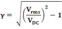
Ripple factor
The ripple factor is given as
Finally, we get
γ = 1.21
Hence, the DC voltage is 121% of the DC magnitude.
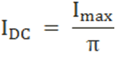
DC current
The DC current is given by,
Where,
Imax = maximum DC load current
Output DC voltage (VDC)
The output DC voltage is given by,
Where, VSmax = Maximum secondary voltage
Rectifier efficiency
It is defined as the ratio of output DC power to the input AC power.
The rectifier efficiency of a half wave rectifier is 40.6%
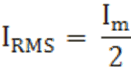
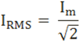
Root mean square (RMS)
The root mean square (RMS) value of load current in a half wave rectifier is

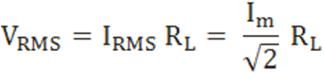
The root mean square (RMS) value of output load voltage in a half wave rectifier is
Form factor
It is defined as the ratio of RMS value to the DC value given by,
F.F = RMS value / DC value
The form factor of a half wave rectifier is F.F = 1.57
Advantages:
- Very few components are used. So, the cost is very low.
- Easy to construct
Disadvantages:
- Loss of power
- Pulsating direct current
- Produces low output voltage.
Key Takeaways:
- It allows only half cycle and blocks the other half cycle.
- When it allows positive half cycles and blocks negative half cycles, it is called a positive half wave rectifier and vice-versa.
Types on the basis of construction:
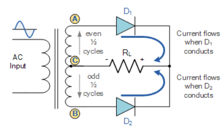
- Center-taped transformer
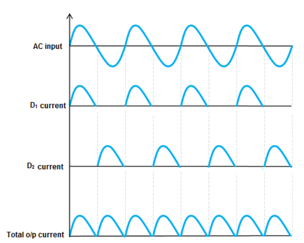
It consists of two power diodes connected to a single load resistance (RL) and each diode supply current to the load one by one. When point A of the transformer becomes positive, diode D1 conducts in the forward direction.
When point B becomes positive (for the negative half of the cycle) with respect to point C, diode D2 conducts and the current starts flowing through resistor R is in the same direction for both half-cycles.
As the output voltage across the resistor R is the sum of the two waveforms combined, this type of circuit is also called as a “bi-phase” circuit.
The spaces present between the frequency response of each half-wave developed by each diode is now being filled in by the other therefore, the average DC output voltage across the load resistor becomes double that of the single half-wave rectifier circuit.

2. Bridge Rectifier
It uses four individual rectifying diodes which are connected in a closed loop called “bridge” configuration to produce the desired output.
It does not require a special centre tapped transformer, hence reducing its size and cost. The single secondary winding is connected one side to the diode bridge network and the other side to the load.
The four diodes D1 to D4 are arranged in “series pairs” and only two diodes conduct current during each half cycle.
During the positive half cycle, diodes D1 and D2 conduct in series while diodes D3 and D4 are reverse biased producing current through the load.
During the negative half cycle, diodes D3 and D4 conduct in series and diodes D1 and D2 are switched “OFF” as they become reverse biased producing current through the load.
During each half cycle the current flows through two diodes instead of just one. The ripple frequency is now twice the supply frequency.
Output Waveform:

Characteristics of full wave rectifier
Ripple factor
The ripple factor is given by
Finally, we get γ = 0.48
Rectifier efficiency
It is defined as the ratio of DC output power to the AC input power.
It can be mathematically written as
η = output PDC / input PAC
The rectifier efficiency of a full wave rectifier is 81.2%.
Peak inverse voltage (PIV)
It is the maximum voltage a diode can withstand in the reverse bias condition.
The peak inverse voltage (PIV) = 2Vsmax
DC output current
The current produced by D1 is Imax / π and the current produced by D2 is Imax / π.
So, the output current IDC = 2Imax / π
Where, Imax = maximum DC load current
DC output voltage
The DC output voltage appeared at the load resistor RL is given as
VDC = 2Vmax /π
Where,
Vmax = maximum secondary voltage
Root mean square (RMS) value of load current IRMS
The root mean square (RMS) value of load current in a full wave rectifier is
The root mean square (RMS) value of output load voltage in a full wave rectifier is
Form factor
It is the ratio of RMS value of current to the DC output current
F.F = RMS value of current / DC output current
The form factor of a full wave rectifier is F.F = 1.11
Advantages :
- High rectifier efficiency
- Low power loss
- Low ripples
- It has fewer ripples than the half wave rectifier.
Disadvantages:
- High cost
- The center tapped transformers are expensive and occupy a large space.
Key Takeaways:
- The process of converting the AC current into DC current is called rectification.
- When an additional wire is connected across the exact middle of the secondary winding of a transformer, it is known as a center tapped transformer.
- Bridge rectifier uses four individual rectifying diodes connected in a closed loop “bridge” configuration to produce the desired output.
Numerical:
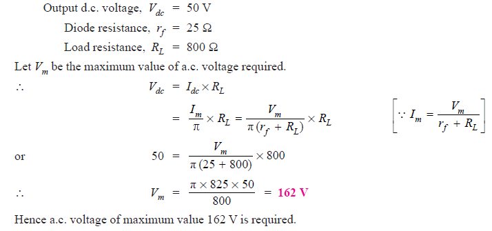
1. A half-wave rectifier is used to supply 50V d.c. To a resistive load of 800 Ω. The
diode has a resistance of 25 Ω. Calculate a.c. Voltage required.
Solution :
2. A full-wave rectifier uses two diodes, the internal resistance of each diode may
be assumed constant at 20 Ω. The transformer r.m.s. Secondary voltage from centre tap to each end of secondary is 50 V and load resistance is 980 Ω. Find : (i) the mean load current (ii) the r.m.s. Value of load current.
Solution :
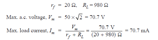
(i) 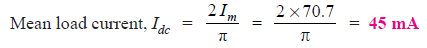
(ii) 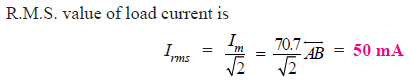
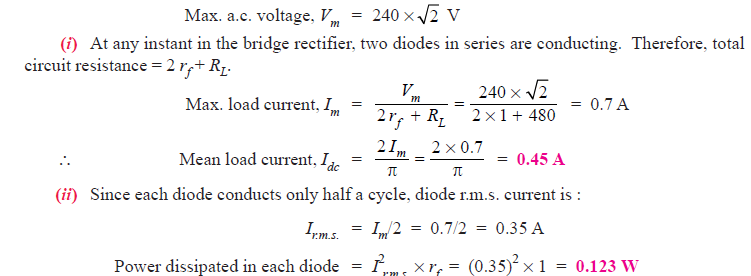
3. The four diodes used in a bridge rectifier circuit have forward resistances which may be considered constant at 1Ω and infinite reverse resistance. The alternating supply voltage is 240 V r.m.s. And load resistance is 480 Ω. Calculate (i) mean load current and (ii) power dissipated in each diode.
Solution :
Line regulation is the ability to maintain specified output voltage over changes in the input line voltage.
Load regulation is the ability to maintain specified output voltage given changes in the load.
Regulation system uses capacitance in order to smooth out the ripples i,e the positive half cycle. This capacitance is also called as smoothing capacitance. The final output will be a straight line above 0.7v (assuming the cut-in voltage is 0.7 because of silicon).
RC circuit consists of resistors and capacitors which allows a certain amount of signal frequency and rejects unwanted signal.
The functioning of circuit depends on the required cut off frequency.
Cut off frequency is the frequency above or below which the output power decreases to the one half the pass band power usually referred to as 3dB point .
Low pass filter is a circuit which passes only low frequency signals and attenuates high frequency signals and it is determined by the RC time constant.
At high frequencies the capacitor offers less amount of reactance and hence the output decreases as frequency increases.
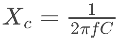
Where Xc=Capacitive reactance measured in ohms, f = frequency in hertz, C = capacitance in farad.
When f = 0 Xc = ∞ (Open Circuit) Xc = 0 (Short Circuit)
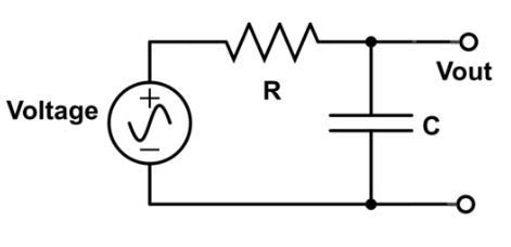
LOW PASS RC CIRCUIT AS AN INTEGRATOR:
An integrator depends upon the time constant of the RC circuit .
The time constant is large enough as compared with the input signal so that the capacitor charges slowly and the input voltage is applied across the resistor.
Here, the output is an integral function of the input voltage and is given by,
The output equation is given by the equation Vo = 1 / c
Frequency Response:

HIGH PASS CIRCUIT AS DIFFERENTIATOR:
The high pass circuit acts as a differentiator depending upon the time constant of the RC network.
It varies depending upon the circuit.
The time constant of the circuit is small and the capacitor charges quickly as all the voltage is taken by the capacitor and small amount of voltage appears across the resistor.
The current in the circuit is decided by the capacitance.

The output equation is given by: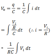
Frequency Response:

Key Takeaways:
- Cut off frequency is the frequency above or below which the output power decreases to the one half the pass band power usually referred to as 3dB point.
- Low pass filter is a circuit which passes only low frequency signals and attenuates high frequency signals when passed through a network over certain cutoff frequency and it is determined by the RC time constant.
Here, inductor L is in series and shunt capacitor C is connected with load.
The choke (L) i.e. inductor allows the dc component to pass through it because its dc resistance R is very small.
It acts as open circuit and the capacitive reactance Xc is very high for dc.
All dc current that passes through dc output voltage is obtained.
The inductive reactance XL = 2pfL is high for ac components.
Therefore, the ripples are reduced.

Waveform:

Advantages:
- In choke input filter, current flows continuously. Therefore, the transformer is used more efficiently.
- Ripple content at the output is low.
- It is less dependent on the load current.
- DC voltage drop across L is much smaller because its de resistance R is very small.
Disadvantages:
- Large size and weight of inductors,
- More cost,
- External hold is produced by inductor.
Key Takeaways:
- The inductive reactance XL = 2pfL is high for ac components.
- Inductor L is in series and shunt capacitor C is connected with load.
It consists of a shunt capacitor and an L-section filter. The output from the rectifier is given across the capacitor.
The DC output voltage is filtered firstly by the capacitor and then by choke coil and then again by another shunt capacitor.
The construction resembles the shape of Greek letter Pi (π). Thus, it is named as Pi filter. It is also called as capacitor input filter.

Working:
It consists of AC components. Thus, it is important to remove these AC ripples to improve the performance of the device. The rectifier output is directly applied to the input capacitor. The capacitor provides low impedance to AC ripples present in the output voltage and high resistance to DC voltage. Hence, most of the AC ripples get bypassed through the capacitor in input stage only.
Here, one inductor and capacitor are present so if some AC ripples say 1% is left after filtering that can be removed in Pi-filter. Thus, Pi filter is considered more efficient.
Characteristics:
It generates a high output voltage at low current drains. The major filtering action is carried by the capacitor at input C1. The residual AC ripples are filtered by inductor coil L and capacitor C2.

Advantages:
- High Output Voltage
- Low Ripple factor
- High PIV
Disadvantage:
- Poor Voltage Regulation
Application:
- In communication devices for retrieving any particular signal after modulation.
Key Takeaways:
- The construction resembles the shape of Greek letter Pi (π). Thus, it is named as Pi filter. It is also called as capacitor input filter.
- If some AC ripples say 1% is left after filtering that can be removed in Pi-filter. Thus, Pi filter is considered more efficient.
CLIPPER
Clippers are networks that employ diodes to “clip” away a portion of an input signal without distorting the remaining part of the applied waveform.
Positive Diode Clipping Circuits
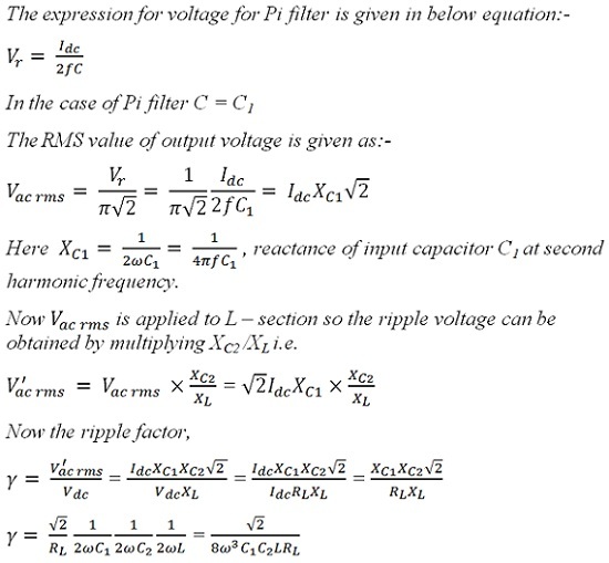
In this, the diode is forward biased during the positive half cycle of the sinusoidal input waveform. For this, it must have the input voltage magnitude greater than +0.7 volts (0.3 volts for a germanium diode).
When this happens, the diodes begins to conduct and holds the voltage across itself until the sinusoidal waveform falls below the value. Thus, the output voltage taken across the diode can never exceed 0.7 volts during the positive half cycle.
During the negative half cycle, the diode is reverse biased blocking current flow through itself and thus has no effect on the negative half of the sinusoidal voltage which passes to the load unaltered. Thus, the diode limits the positive half of the input waveform and is known as a positive clipper circuit.
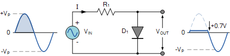
Negative Diode Clipping Circuits
Here the reverse happens. The diode is forward biased during the negative half cycle of the sinusoidal waveform and limits or clips it to –0.7 volts while allowing the positive half cycle to pass unaltered when reverse biased.
As the diode limits the negative half cycle of the input voltage it is therefore called a negative clipper circuit.
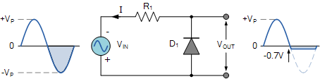
Clipping of Both Half Cycles
If the two diodes are connected in inverse parallel, then both the positive and negative half cycles would be clipped as diode D1 clips the positive half cycle of the sinusoidal input waveform while diode D2 clips the negative half cycle.
Hence, diode clipping circuits can be used to clip the positive half cycle, the negative half cycle or both.
For ideal diodes the output waveform above would be zero. However, due to the forward bias voltage drop across the diodes the actual clipping point occurs at +0.7 volts and –0.7 volts respectively.
Applications:
- To modify an input waveform using signal and Schottky diodes.
- To provide over-voltage protection using zener diodes
- For voltage limiting.
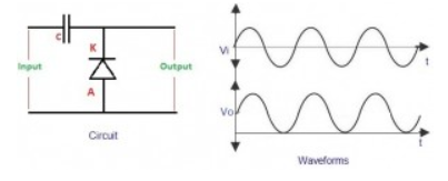
CLAMPER
A clamper is a network constructed of a diode, a resistor, and a capacitor that shifts a waveform to a different dc level without changing the appearance of the applied signal.
The positive or negative peak of a signal can be positioned at the desired level by using the clamping circuits. As we can shift the levels of peaks of the signal by using a clamper, hence, it is also called as level shifter.
The clamper circuit consists of a capacitor and diode connected in parallel across the load. The clamper circuit depends on the change in the time constant of the capacitor. The capacitor must be chosen such that, during the conduction of the diode, the capacitor must be sufficient to charge quickly and during the non-conducting period of diode, the capacitor should not discharge drastically. The clampers are classified as positive and negative clampers based on the clamping method.
Negative Clamper

During the positive half cycle, the input diode is in forward bias and as the diode conducts, capacitor gets charged. During the negative half cycle, the output voltage become equal to the sum of the input voltage and the voltage stored across the capacitor.
Positive Clamper
It is similar to the negative clamper circuit, but the diode is connected in the opposite direction. During the positive half cycle, the voltage across the output terminals becomes equal to the sum of the input voltage and capacitor voltage. During the negative half cycle, the diode starts conducting and charges the capacitor rapidly to its peak input value. Thus, the waveforms are clamped towards the positive direction.
Applications:
- They are used in test equipment, sonar and radar systems.
- For the protection of the amplifiers from large errant signals clampers are used.
- For removing the distortions.
- For improving the overdrive recovery time.
- As voltage doublers or voltage multipliers.
Key Takeaways:
- A clamper is a network constructed of a diode, a resistor, and a capacitor that shifts a waveform to a different dc level without changing the appearance of the applied signal.
- Clippers are networks that employ diodes to “clip” away a portion of an input signal without distorting the remaining part of the applied waveform.
Voltage-multiplier circuits are employed to maintain a relatively low transformer peak voltage while stepping up the peak output voltage to two, three, four, or more times the peak rectified voltage.
Voltage Doubler
During the positive half cycle, secondary diode D 1 conducts (and diode D 2 is cut off), charging capacitor C 1 up to the peak rectified voltage ( V m ). Diode D 1 is short and the input voltage capacitor C 1 charges to V m. During the negative half-cycle, diode D 1 is cut off and diode D 2 conducts and charges capacitor C 2 . Since diode D 2 acts for a short time during the negative half-cycle, the voltages around the outside loop is:
-Vm - VC1 + VC2 = 0
-Vm - Vm + VC2 = 0
VC2 = 2Vm


For the positive half-cycle, diode D 2 does not conduct and capacitor C 2 discharges through the load. If no load is connected across capacitor C 2 , both capacitors stay charged— C 1 to V m and C 2 to 2 V m . The peak inverse voltage across each diode is 2 V m .
Key Takeaways:
- Voltage-multiplier circuits are employed to maintain a relatively low transformer peak voltage while stepping up the peak output voltage to two, three, four, or more times the peak rectified voltage.
References:
1 “Electronic devices and circuit theory” by Boylestead and Nashelsky, Pearson
2 “Electronic principle” by Albert Malvino and Davis J Bates, TMH
3 “Integrated Electronics”, By Jacob Millman and Christos Halkias


