Unit 3
Semiconductor
A semiconductor is a substance whose resistivity lies between the conductors and insulators. The property of resistivity is not the only one that decides a material as a semiconductor, but it has few properties as follows.
- Semiconductors have the resistivity which is less than insulators and more than conductors.
- Semiconductors have negative temperature co-efficient. The resistance in semiconductors, increases with the decrease in temperature and vice versa.
- The Conducting properties of a Semiconductor changes, when a suitable metallic impurity is added to it, which is a very important property.
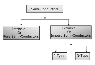
Semiconductor devices are extensively used in the field of electronics. The transistor has replaced the bulky vacuum tubes, from which the size and cost of the devices got decreased and this revolution has kept on increasing its pace leading to the new inventions like integrated electronics. The following illustration shows the classification of semiconductors.
|
Conduction in Semiconductors
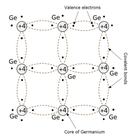
After having some knowledge on the electrons, we came to know that the outermost shell has the valence electrons which are loosely attached to the nucleus. Such an atom, having valence electrons when brought close to the other atom, the valence electrons of both these atoms combine to form “Electron pairs”. This bonding is not so very strong and hence it is a Covalent bond.
For example, a germanium atom has 32 electrons. 2 electrons in first orbit, 8 in second orbit, 18 in third orbit, while 4 in last orbit. These 4 electrons are valence electrons of germanium atom. These electrons tend to combine with valence electrons of adjoining atoms, to form the electron pairs, as shown in the following figure.
|
Creation of Hole
Due to the thermal energy supplied to the crystal, some electrons tend to move out of their place and break the covalent bonds. These broken covalent bonds, result in free electrons which wander randomly. But the moved away electrons creates an empty space or valence behind, which is called as a hole.
This hole which represents a missing electron can be considered as a unit positive charge while the electron is considered as a unit negative charge. The liberated electrons move randomly but when some external electric field is applied, these electrons move in opposite direction to the applied field. But the holes created due to absence of electrons, move in the direction of applied field.
Hole Current
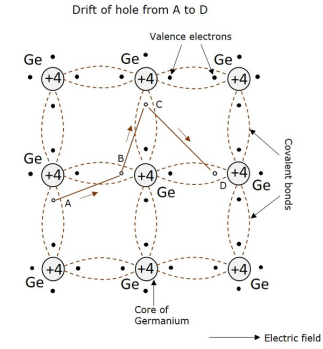
It is already understood that when a covalent bond is broken, a hole is created. Actually, there is a strong tendency of semiconductor crystal to form a covalent bond. So, a hole doesn’t tend to exist in a crystal. This can be better understood by the following figure, showing a semiconductor crystal lattice.
|
An electron, when gets shifted from a place A, a hole is formed. Due to the tendency for the formation of covalent bond, an electron from B gets shifted to A. Now, again to balance the covalent bond at B, an electron gets shifted from C to B. This continues to build a path. This movement of hole in the absence of an applied field is random. But when electric field is applied, the hole drifts along the applied field, which constitutes the hole current. This is called as hole current but not electron current because, the movement of holes contribute the current flow.
Electrons and holes while in random motion, may encounter with each other, to form pairs. This recombination results in the release of heat, which breaks another covalent bond. When the temperature increases, the rate of generation of electrons and holes increase, thus rate of recombination increases, which results in the increase of densities of electrons and holes. As a result, conductivity of semiconductor increases and resistivity decreases, which means the negative temperature coefficient.
Intrinsic Semiconductors
A Semiconductor in its extremely pure form is said to be an intrinsic semiconductor. The properties of this pure semiconductor are as follows −
- The electrons and holes are solely created by thermal excitation.
- The number of free electrons is equal to the number of holes.
- The conduction capability is small at room temperature.
In order to increase the conduction capability of intrinsic semiconductor, it is better to add some impurities. This process of adding impurities is called as Doping. Now, this doped intrinsic semiconductor is called as an Extrinsic Semiconductor.
Doping
The process of adding impurities to the semiconductor materials is termed as doping. The impurities added, are generally pentavalent and trivalent impurities.
Pentavalent Impurities
- The pentavalent impurities are the ones which has five valence electrons in the outer most orbit. Example: Bismuth, Antimony, Arsenic, Phosphorus
- The pentavalent atom is called as a donor atom because it donates one electron to the conduction band of pure semiconductor atom.
Trivalent Impurities
- The trivalent impurities are the ones which has three valence electrons in the outer most orbit. Example: Gallium, Indium, Aluminum, Boron
- The trivalent atom is called as an acceptor atom because it accepts one electron from the semiconductor atom.
Extrinsic Semiconductor
An impure semiconductor, which is formed by doping a pure semiconductor is called as an extrinsic semiconductor. There are two types of extrinsic semiconductors depending upon the type of impurity added. They are N-type extrinsic semiconductor and P-Type extrinsic semiconductor.
N-Type Extrinsic Semiconductor
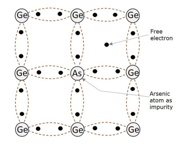
A small amount of pentavalent impurity is added to a pure semiconductor to result in Ntype extrinsic semiconductor. The added impurity has 5 valence electrons.
For example, if Arsenic atom is added to the germanium atom, four of the valence electrons get attached with the Ge atoms while one electron remains as a free electron. This is as shown in the following figure.
|
All of these free electrons constitute electron current. Hence, the impurity when added to pure semiconductor, provides electrons for conduction.
- In N-type extrinsic semiconductor, as the conduction takes place through electrons, the electrons are majority carriers and the holes are minority carriers.
- As there is no addition of positive or negative charges, the electrons are electrically neutral.
- When an electric field is applied to an N-type semiconductor, to which a pentavalent impurity is added, the free electrons travel towards positive electrode. This is called as negative or N-type conductivity.
P-Type Extrinsic Semiconductor
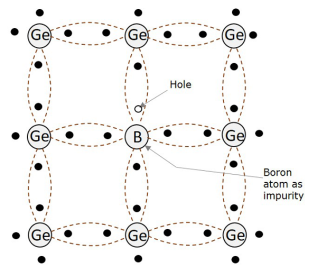
A small amount of trivalent impurity is added to a pure semiconductor to result in P-type extrinsic semiconductor. The added impurity has 3 valence electrons. For example, if Boron atom is added to the germanium atom, three of the valence electrons get attached with the Ge atoms, to form three covalent bonds. But, one more electron in germanium remains without forming any bond. As there is no electron in boron remaining to form a covalent bond, the space is treated as a hole. This is as shown in the following figure.
|
The boron impurity when added in a small amount, provides a number of holes which helps in the conduction. All of these holes constitute hole current.
- In P-type extrinsic semiconductor, as the conduction takes place through holes, the holes are majority carriers while the electrons are minority carriers.
- The impurity added here provides holes which are called as acceptors, because they accept electrons from the germanium atoms.
- As the number of mobile holes remains equal to the number of acceptors, the Ptype semiconductor remains electrically neutral.
- When an electric field is applied to a P-type semiconductor, to which a trivalent impurity is added, the holes travel towards negative electrode, but with a slow pace than electrons. This is called as P-type conductivity.
- In this P-type conductivity, the valence electrons move from one covalent bond to another, unlike N-type.
Why Silicon is Preferred in Semiconductors?
Among the semiconductor materials like germanium and silicon, the extensively used material for manufacturing various electronic components is Silicon SiSi. Silicon is preferred over germanium for many reasons such as −
- The energy band gap is 0.7ev, whereas it is 0.2ev for germanium.
- The thermal pair generation is smaller.
- The formation of SiO2 layer is easy for silicon, which helps in the manufacture of many components along with integration technology.
- Si is easily found in nature than Ge.
- Noise is less in components made up of Si than in Ge.
Hence, Silicon is used in the manufacture of many electronic components, which are used to make different circuits for various purposes. These components have individual properties and particular uses.
Diode Equivalent Circuits
Diode is an active element in electrical circuit it has some resistance and some value of junction capacitance when the diode in circuit is replaced by same value of the resistance and capacitance its called as the Diode equivalent circuit.
To define the dc diode model, we look at the characteristics of an ideal diode and the modifications that were required due to practical considerations. To review: ¾ Ideal diode: VON = 0, Rr = ∞ and Rf = 0. In other words, the ideal diode is a short in the forward bias region and an open in the reverse bias region. ¾ Practical diode (silicon): VON = 0.7V, Rr < ∞ (typically several MΩ), Rf ≈ rd (typically < 50 Ω). The general representation for a practical diode under dc operating conditions is shown below. Recall the diode is a two-terminal device, which simply means that it connects to other circuit elements at connection points labeled a and b in the circuit below with the voltage Vab applied across the diode. Note that the terminal voltage Vab is the same as the voltage applied across the diode, vD – same animal, different notation. This model may be simplified if we can define the operating region as forward or reverse bias. For the forward bias region (vD ≥ 0.7 V for silicon), the ideal diode is a short and the terminal characteristics of the model above reduce to the parallel combination of Rr and Rf. Since Rr >> Rf, Rr ||Rf ≈ Rf. Likewise, when the voltage applied to the diode is less than VON (vD < 0.7 V for silicon), the ideal diode is an open and the resistance between terminals a and b is Rr. These two cases are illustrated below for reference
|
Even though the same, they behave very differently! Remember the values of the resistances in the different regions and you can see that diode characteristics in the forward and reverse bias regions are quite distinct.
Diode Characteristics
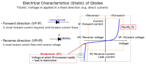
Basic static characteristics of diodes are the forward voltage VF and forward current IF, and the reverse voltage and current VR and IR.
The area surrounded by the orange dashed line in the diagram on the right indicates the usable area of rectifying diodes. Specifically, this is the area within the range of allowable IF, and within the breakdown voltage range in the reverse direction.
It should be noted that the area enclosed by the green dashed line is the usable area of Zener diodes, although these are not discussed in this chapter. This area isn’t usable for other diodes, and if this area is entered without any limits on the IR, device failure may occur.
|
Diode as a Switch
Whenever a specified voltage is exceeded, the diode resistance gets increased, making the diode reverse biased and it acts as an open switch. Whenever the voltage applied is below the reference voltage, the diode resistance gets decreased, making the diode forward biased, and it acts as a closed switch.
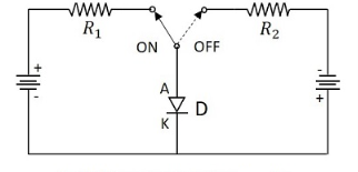
The following circuit explains the diode acting as a switch.
|
A switching diode has a PN junction in which P-region is lightly doped and N-region is heavily doped. The above circuit symbolizes that the diode gets ON when positive voltage forward biases the diode and it gets OFF when negative voltage reverse biases the diode.
As the forward current flows till then, with a sudden reverse voltage, the reverse current flows for an instance rather than getting switched OFF immediately. The higher the leakage current, the greater the loss. The flow of reverse current when the diode is reverse biased suddenly may sometimes create few oscillations, called RINGING.
This ringing condition is a loss and hence should be minimized. To do this, the switching times of the diode should be understood.
Diode as a Rectifier (half-wave & full-wave)
A complete half-wave rectifier circuit consists of 3 main parts:
- A transformer
- A resistive load
- A diode
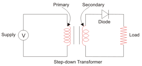
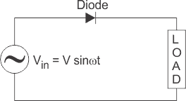
A half wave rectifier circuit diagram looks like this:
|
First, a high AC voltage is applied to the to the primary side of the step- down transformer and we will get a low voltage at the secondary winding which will be applied to the diode.
|
During the positive half cycle of the AC voltage, the diode will be forward biased and the current flows through the diode. During the negative half cycle of the AC voltage, the diode will be reverse biased and the flow of current will be blocked. The final output voltage waveform on the secondary side (DC) is shown in figure above.
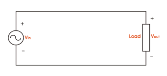
If we replace the secondary transformer coils with a source voltage, we can simplify the circuit diagram of the half-wave rectifier as:
|
For the positive half cycle of the AC source voltage, the equivalent circuit effectively becomes:
|
This is because the diode is forward biased, and is hence allowing current to pass through. So, we have a closed circuit.
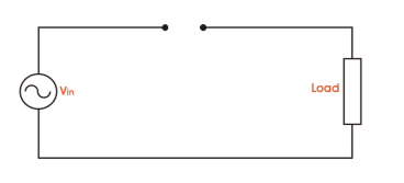
But for the negative half cycle of the AC source voltage, the equivalent circuit becomes:
|
Because the diode is now in reverse bias mode, no current is able to pass through it. As such, we now have an open circuit. Since current cannot flow through to the load during this time, the output voltage is equal to zero.
This all happens very quickly – since an AC waveform will oscillate between positive and negative many times each second (depending on the frequency).
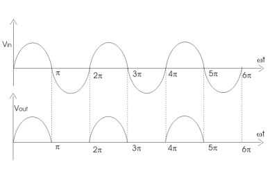
Here’s what the half wave rectifier waveform looks like on the input side (Vin), and what it looks like on the output side (Vout) after rectification (i.e. conversion from AC to DC):
|
The graph above actually shows a positive half wave rectifier. This is a half-wave rectifier which only allows the positive half-cycles through the diode,and blocks the negative half-cycle.
The voltage waveform before and after a positive half wave rectifier is shown in figure 4 below.
|
Conversely, a negative half-wave rectifier will only allow negative half-cycles through the diode and will block the positive half-cycle. The only difference between a posive and negative half wave rectifier is the direction of the diode.
As you can see in figure 5 below, the diode is now in the opposite direction. Hence the diode will now be forward biased only when the AC waveform is in its negative half cycle.
|
ADVANTAGES:-
1)Simple Construction.
2) Component required less.
3)Small size.
APPLICATION:-
Walkman, low-cost power supply.
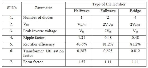
TRANSFORMER UTILISATION FACTOR(TUF): It indicates how well the ilp transformer is being utilized TUF= DC O/P Power / AC power rating of the transformer
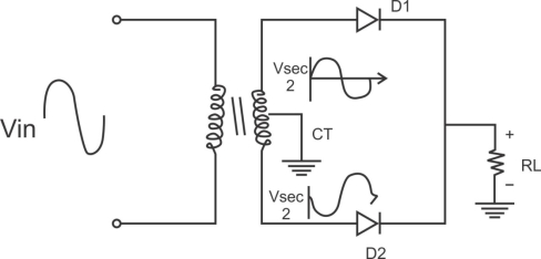
Full wave rectifier 1) A center-tapped rectifier is a type of full-wave rectifier that uses two diodes connected to the secondary of a center-tapped transformer.
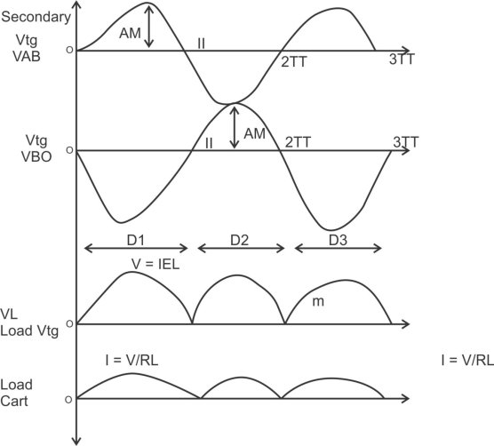
Center tapped full wave rectifier operation:- I) During the positive half cycle of the i/p ac supply. diagram
D1.Is in forward biased & D2 is in reverse biased. II)During -ve half cycle.
D1 Reverse biased D2 Forward biased
|
ADVANTAGES
- Law ripple factor as Compared to HKR.
- Better rectification efficiency.
- Better TUF.
- A higher value of average load vtg & avg load crt.
- No possibility of transformer core saturation.
DISADVANTAGES
PIV of the diode is 2vm, more size costly.
APPLICATION
I) Battery charges.
2)power supply at the laboratory, high current, electronic ckt.
Capacitor filter
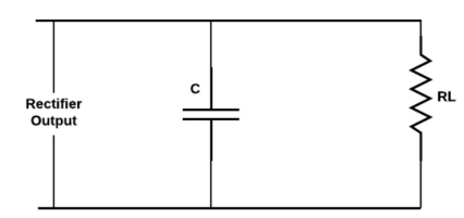
A typical capacitor filter circuit diagram is shown below. The designing of this circuit can be done with a capacitor C as well as load resistor (RL). The rectifier’s exciting voltage is given across the terminals of a capacitor. Whenever the voltage of the rectifier enhances then the capacitor will be charged as well as supplies the current to the load.
|
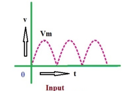
At the last part of the quarter phase, the capacitor will be charged to the highest rectifier voltage value that is denoted with Vm, and then the voltage of the rectifier starts to reduce. As this happens, the capacitor starts discharging through the voltage across it and load. The voltage across the load will reduce little only because the next peak voltage occurs instantaneously to charge the capacitor. This procedure will repeat many times and the output waveform will be seen that very slight ripple is missing in the output. Furthermore, the output voltage is superior because it remains significantly close to the highest value of the output voltage of the rectifier.
|
|
The following two processes cause junction breakdown due to the increase in reverse bias voltage.
(i) Zener Breakdown
(ii) Avalanche Breakdown
Zener Breakdown
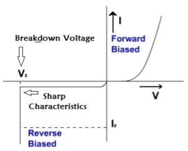
The Zener Breakdown is observed in the Zener diodes having Vz less than 5V or between 5 to 8 volts. When a reverse voltage is applied to a Zener diode, it causes a very intense electric field to appear across a narrow depletion region. Such an intense electric field is strong enough to pull some of the valence electrons into the conduction band by breaking their covalent bonds .these electrons then become free electrons which are available for conduction. A large number of such free electrons will constitute a large reverse current through the Zener diode and breakdown is said to have occurred due to the Zener effect.
Characteristics of Zener Breakdown is shown below:
Zener Breakdown Characteristics |
A current limiting resistance should be connected in series with the Zener diode to protect it against the damage due to excessive heating. In Zener breakdown, the breakdown voltage depends on the temperature of P-N junction.The breakdown voltage decreases with increase in the junction temperature.
Avalanche Breakdown
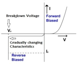
The avalanche breakdown is observed in the Zener Diodes having Vz having than 8 V. In the reverse biased condition, the conduction will take place only due to the minority carriers. As we increase the reverse voltage applied to the Zener diode, these minority carriers tend to accelerated. Therefore, the kinetic energy associated with them increases. While travelling, these accelerated minority carriers will collide with the stationary atoms and impart some of the kinetic energy to the valence electrons present in the covalent bonds.
Characteristics of Avalanche Breakdown is shown below:
Avalanche Breakdown Characteristics |
Due to this additionally acquired energy, these valence electrons will break their covalent bonds and jump into the conduction bond to become free conduction. Now these newly generated free electrons will get accelerated. They will knock out some more valence electrons by means of collision. This phenomenon is called as carrier multiplication.
- Zenor diode is a special type of p-n junction semiconductor diode in this diode the reverse breakdown voltage is adjusted precisely between 3v to 200v.
- Its applications are based on this principle hence zenor diode is called as a breakdown diode.
- The doping level of the imparity added to manufacture the zener diode is controlled in order to adjust the precise value of breakdown voltage.
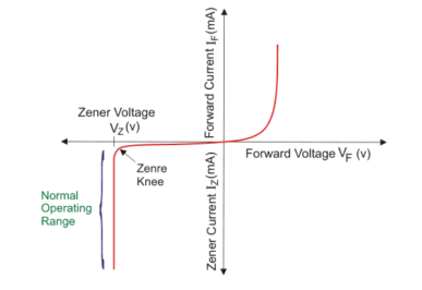
- A graph of current through vs the voltage across the device is called the characteristic of Zener diode.
- The first quadrant is the forward biased region. Here the Zener diode acts like an ordinary diode.
- When a forward voltage is applied, current flows through it. But due to higher doping concentration, higher current flows through the Zener diode
- In the third quadrant, the magic happens. The graph shows the current vs voltage curve when we apply a reverse bias to the diode.
- The Zener breakdown voltage is the reverse bias voltage after which a significant amount of current starts flowing through the Zener diode.
- Here in the diagram, VZ refers to the Zener breakdown voltage. Until the voltage reaches Zener breakdown level, tiny amount of current flows through the diode. Once the reverse bias voltage becomes more than the Zener breakdown voltage, a significant amount of current starts flowing through the diode due to Zener breakdown.
- The voltage remains at the Zener breakdown voltage value, but the current through the diode increases when the input voltage gets increased. Due to the unique property of Zener diode, the depletion region regains its original position when the reverse voltage gets removed.
- The Zener diode doesn’t get damaged despite this massive amount of current flowing through it.
APPLICATIONS:
Zener diodes are used for voltage regulation, as reference elements, surge suppressors, and in switching applications and clipper circuits.
PHOTODIODE:
|
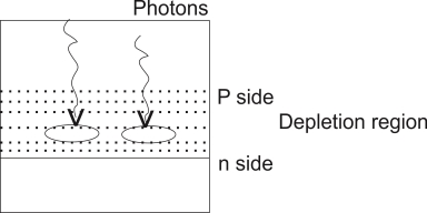
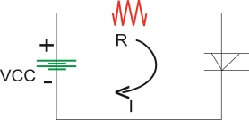
The light is always focused through a glass lens on the junction of the photodiode As the photodiode is reverse biased the depletion region is quite wide, penetrated on both sides of the junction.
The photons incident on the depletion region will impact their energy to the Ions present in the depletion region and generates e hole pairs.
The photons incident on the depletion region, so the number of electron hole pairs will be generated, depends on the intensity of light [number of photons] These and holes will be attracted towards the +ve & -ve terminals respectively of the photocurrent.
With an increase in the light intensity more number of e hole pairs are generated and the photocurrent increases thus the photocurrent is proportional to the light intensity.
LED:
|
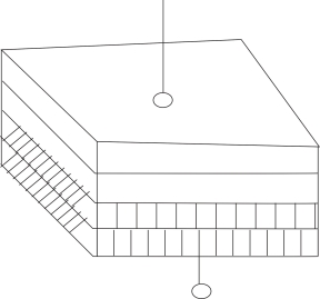
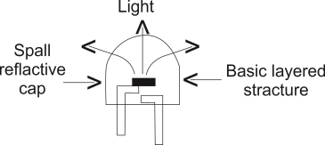
Construction of LED:-
To make the emission of light in one direction cup type construction is used for LED.
|
PRINCIPLE LED OPERATION
When the led is forward biased the electrons in the n-region will cross the junction and recombine with the holes in the p-type material.
These free e- reside in the conduction band & hence at a higher energy level than the holes in the valence band
When recombination takes place this e- return peak to the valence band which is at a lower energy level than the conduction band.
while returning back the recombining e-give away the excess energy in the form of light. This process is called electroluminescence. in this way an LED emits light.
Color of the Emitted Light
Material Use Color of Emitted Light
i) Gallium Arsenide (GOAS) In fared (IR)
ii) GaASP(gallium arsenide Red or Yellow
phosphide)
iii) Gallium phosphide (GAP) Red or Green
Application
Used in 7 Segment Display
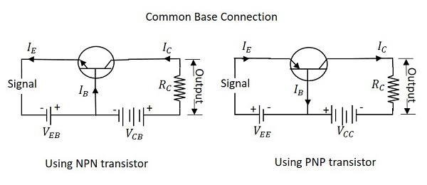
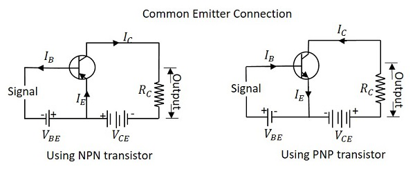
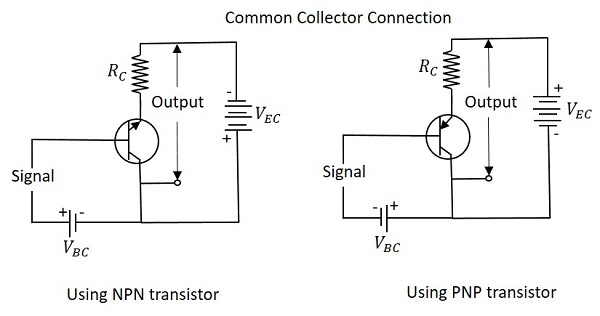
The three types of configurations are Common Base, Common Emitter and Common Collector configurations. In every configuration, the emitter junction is forward biased and the collector junction is reverse biased.
The name itself implies that the Base terminal is taken as common terminal for both input and output of the transistor. The common base connection for both NPN and PNP transistors is as shown in the following figure.
For the sake of understanding, let us consider NPN transistor in CB configuration. When the emitter voltage is applied, as it is forward biased, the electrons from the negative terminal repel the emitter electrons and current flows through the emitter and base to the collector to contribute collector current. The collector voltage VCB is kept constant throughout this. In the CB configuration, the input current is the emitter current IE and the output current is the collector current IC. Current Amplification Factor α The ratio of change in collector current ΔIC to the change in emitter current ΔIE when collector voltage VCB is kept constant, is called as Current amplification factor. It is denoted by α. α=ΔIC/ΔIE atconstantVCB Expression for Collector current Along with the emitter current flowing, there is some amount of base current IB which flows through the base terminal due to electron hole recombination. As collector-base junction is reverse biased, there is another current which is flown due to minority charge carriers. This is the leakage current which can be understood as Ileakage. This is due to minority charge carriers and hence very small. The emitter current that reaches the collector terminal is αIE Total collector current IC=αIE+Ileakage If the emitter-base voltage VEB = 0, even then, there flows a small leakage current, which can be termed as ICBO collector−basecurrentwithoutputopencollector−basecurrentwithoutputopen. The collector current therefore can be expressed as IC=αIE+ICBO IE=IC+IB IC=α(IC+IB)+ICBO IC(1−α)=αIB+ICBO IC=(α1−α)IB+(ICBO1−α) IC=(α1−α)IB+(11−α)ICBO Hence the above derived is the expression for collector current. The value of collector current depends on base current and leakage current along with the current amplification factor of that transistor in use. Characteristics of CB configuration
η=ΔVEB/ΔIE atconstantVCB
ro=ΔVCB/ΔIC atconstant lE
Common Emitter CE
Just as in CB configuration, the emitter junction is forward biased and the collector junction is reverse biased. The flow of electrons is controlled in the same manner. The input current is the base current IB and the output current is the collector current IC here. Base Current Amplification factor β The ratio of change in collector current ΔIC to the change in base current ΔIB is known as Base Current Amplification Factor. It is denoted by β β=ΔICΔ/IB Relation between β and α Let us try to derive the relation between base current amplification factor and emitter current amplification factor. β=ΔIC/ΔIB α=ΔIC/ΔIE IE=IB+IC ΔIE=ΔIB+ΔIC ΔIB=ΔIE−ΔIC We can write β=ΔIC/ΔIE−ΔIC Dividing by ΔIE
β=ΔIC/ΔIE/ΔIE/ΔIE−ΔIC/ΔIE We have α=ΔIC/ΔIE Therefore, β=α/1−α From the above equation, it is evident that, as α approaches 1, β reaches infinity. Hence, the current gain in Common Emitter connection is very high. This is the reason this circuit connection is mostly used in all transistor applications. Expression for Collector Current In the Common Emitter configuration, IB is the input current and IC is the output current. We know IE=IB+IC And IC=αIE+ICBO =α(IB+IC)+ICBO IC(1−α)=αIB+ICBO IC=α/1−α IB+1/1−α ICBO If base circuit is open, i.e. if IB = 0, The collector emitter current with base open is ICEO ICEO=1/1−αICBO Substituting the value of this in the previous equation, we get IC=α/1−α . IB+ ICEO IC=βIB+ICEO Hence the equation for collector current is obtained. Knee Voltage In CE configuration, by keeping the base current IB constant, if VCE is varied, IC increases nearly to 1v of VCE and stays constant thereafter. This value of VCE up to which collector current IC changes with VCE is called the Knee Voltage. The transistors while operating in CE configuration, they are operated above this knee voltage. Characteristics of CE Configuration
ri=ΔVBE/ΔIB at constant VCE
ro=ΔVCE/ΔIC at constant IB
Common Collector CC Configuration The name itself implies that the Collector terminal is taken as common terminal for both input and output of the transistor. The common collector connection for both NPN and PNP transistors is as shown in the following figure.
Just as in CB and CE configurations, the emitter junction is forward biased and the collector junction is reverse biased. The flow of electrons is controlled in the same manner. The input current is the base current IB and the output current is the emitter current IE here. Current Amplification Factor γ The ratio of change in emitter current ΔIE to the change in base current ΔIB is known as Current Amplification factor in common collector CC configuration. It is denoted by γ. γ=ΔIE/ΔIB
Relation between γ and α Let us try to draw some relation between γ and α γ=ΔIE/ΔIB α=ΔIC/ΔIE IE=IB+IC ΔIE=ΔIB+ΔIC ΔIB=ΔIE−ΔIC Substituting the value of IB, we get γ=ΔIE/ΔIE−ΔIC Dividing by ΔIEΔIE γ=ΔIE/ΔIE/ΔIE/ΔIE−ΔIC/ΔIE 1/1−α1 γ=1/1−α Expression for collector current We know IC=αIE+ICBOIC=αIE+ICBO IE=IB+IC=IB+(αIE+ICBO)IE=IB+IC=IB+(αIE+ICBO) IE(1−α)=IB+ICBOIE(1−α)=IB+ICBO IE=IB1−α+ICBO1−αIE=IB1−α+ICBO1−α IC≅IE=(β+1)IB+(β+1)ICBO The above is the expression for collector current. Characteristics of CC Configuration
|
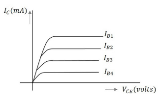
When the output characteristics of a transistor are considered, the curve looks as below for different input values.
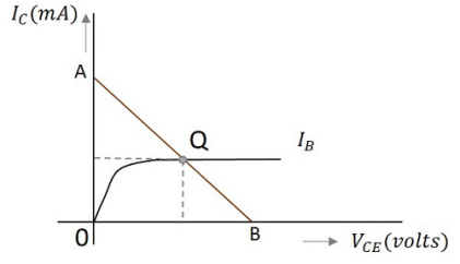
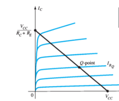
In the above figure, the output characteristics are drawn between collector current IC and collector voltage VCE for different values of base current IB. These are considered here for different input values to obtain different output curves. Operating point When a value for the maximum possible collector current is considered, that point will be present on the Y-axis, which is nothing but the saturation point. As well, when a value for the maximum possible collector emitter voltage is considered, that point will be present on the X-axis, which is the cutoff point. When a line is drawn joining these two points, such a line can be called as Load line. This is called so as it symbolizes the output at the load. This line, when drawn over the output characteristic curve, makes contact at a point called as Operating point. This operating point is also called as quiescent point or simply Q-point. There can be many such intersecting points, but the Q-point is selected in such a way that irrespective of AC signal swing, the transistor remains in active region. This can be better understood through the figure below.
The load line has to be drawn in order to obtain the Q-point. A transistor acts as a good amplifier when it is in active region and when it is made to operate at Q-point, faithful amplification is achieved. Faithful amplification is the process of obtaining complete portions of input signal by increasing the signal strength. This is done when AC signal is applied at its input. This is discussed in AMPLIFIERS tutorial. DC Load line
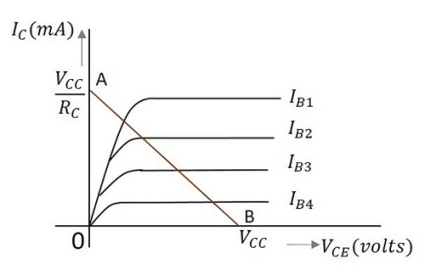
The value of collector emitter voltage at any given time will be VCE=VCC−ICRC As VCC and RC are fixed values, the above one is a first degree equation and hence will be a straight line on the output characteristics. This line is called as D.C. Load line. The figure below shows the DC load line.
To obtain the load line, the two end points of the straight line are to be determined. Let those two points be A and B. To obtain A When collector emitter voltage VCE = 0, the collector current is maximum and is equal to VCC/RC. This gives the maximum value of VCE. This is shown as VCE=VCC−ICRC 0=VCC−ICRC IC=VCC/RC This gives the point A (OA = VCC/RC) on collector current axis, shown in the above figure. To obtain B When the collector current IC = 0, then collector emitter voltage is maximum and will be equal to the VCC. This gives the maximum value of IC. This is shown as VCE=VCC−ICRC =VCC (As IC = 0) This gives the point B, which means (OB = VCC) on the collector emitter voltage axis shown in the above figure. Hence, we got both the saturation and cutoff point determined and learnt that the load line is a straight line. So, a DC load line can be drawn. |
Approximate analysis
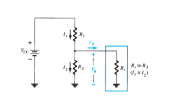
VB = R2 Vcc/ R1 + R2
IE = V E / RE
Ri = (β + 1) RE ͌ β RE
β RE ≥ 10 R2
ICQ = IE
VE = VB – VBE
VCEQ = Vcc – Ic(RC + RE)
Transistor Analysis
IC sat = IC max = Vcc/ Rc + RE
Load Line Analysis
Ic = Vcc/ Rc + RE | Vce =0V
VCE = VCC| Ic =0mA
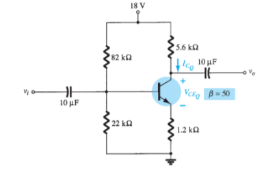
Determine the levels of ICQ and VCEQ for voltage divider configuration using exact and approximate techniques and compare solutions.
β . RE ≥ 10 R2
(50)(1.2 k Ω) ≥ 10(22 k Ω)
Rth = R1 || R2 82 kΩ || 22 kΩ = 17.35 kΩ
Eth = R2 Vcc/ R1 + R2 = 22kΩ (18V)/ 82kΩ + 22kΩ = 3.81 V IB = Eth – VBE/ Rth + (β +1) RE = 3.81 V – 0.7V / 17.35 kΩ + (51 )(1.2kΩ) = 3.11/ 78.55 kΩ = 39.6 μ A
ICQ = β IB = (50)(39.6μA) = 1.98 mA
VCEQ = Vcc – IC(RC + RE)
= 18V – (1.98mA)(5.6kΩ + 1.2 kΩ)= 4.54V
BJT Amplifier
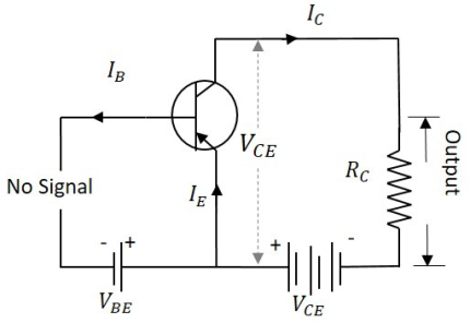
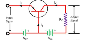
Transistor raises the strength of a weak signal and hence acts an amplifier. The transistor amplifier circuit is shown in the figure below. Transistor as an Amplifier Vee is applied to the input circuit along with the input signal to achieve the amplification. The DC voltage VEE keeps the emitter-base junction under the forward biased condition regardless of the polarity of the input signal and is known as bias voltage. When a weak signal is applied to the input, a small change in signal voltage causes a change in emitter current this change is almost the same in collector current because of the transmitter action. In the collector circuit, a load resistor RC of high value is connected. When collector current flows through such a high resistance, it produces a large voltage drop across it. Thus, a weak signal (0.1V) applied to the input circuit appears in the amplified form (10V) in the collector circuit. Input Resistance When the input circuit is forward biased, the input resistance will be low. The input resistance is the opposition offered by the base-emitter junction to the signal flow. Hence, it is the ratio of small change in base-emitter voltage (ΔVBE) to the resulting change in base current (ΔIB) at constant collector-emitter voltage. Input resistance, Ri=ΔVBE/ΔIb Where Ri = input resistance, VBE = base-emitter voltage, and IB = base current.
Output Resistance The output resistance of a transistor amplifier is very high. The collector current changes very slightly with the change in collector-emitter voltage. The ratio of change in collector-emitter voltage (ΔVCE) to the resulting change in collector current (ΔIC) at constant base current. Output resistance = Ro=ΔVCE/ΔIC Where Ro = Output resistance, VCE = Collector-emitter voltage, and IC = Collector-emitter voltage. Current gain It is the ratio of change in collector current (ΔIC) to the change in base current (ΔIB). Current gain, β=ΔIC/ ΔIB Voltage Gain It is the ratio of change in output voltage (ΔVCE) to the change in input voltage (ΔVBE).
Voltage gain, AV=ΔVCE/ΔVBE
= ΔIC x RAC / ΔIB x Ri = ΔIC / ΔIB x RAC / Ri = β x R AC/ Ri
Power Gain It is the ratio of output signal power to the input signal power. Power gain Ap = (ΔIC) 2 x RAC / (ΔIB ) 2 x Ri = (ΔIC / ΔIB) x ΔIC x RAC / ΔIB x Ri = current gain x voltage gain |
Reference Books:
1. V. N. Mittal, Arvind Mittal, ‘Basic Electrical Engineering’, Tata McGraw Hill publishing co. ltd, New Delhi.
2. D. P. Kothari, I.J Nagrath, ‘Basic Electrical Engineering’, Tata McGraw Hill
3. M. S. Naidu, S. Kamakshaiah, ‘Introduction to Electrical Engineering’, Tata McGraw Hill.
4. P. Tiwari, ‘Basic Electrical Engineering’, New Age Publication.
5. Vincent Del Toro, ‘Electrical Engineering Fundamentals’, Pearson
6. R. P. Jain, ‘Modern Digital Electronics’ McGraw Hill Education (India) Private Limited, Fourth Edition, 2017.
7. B. L. Theraja, ‘Applied Electronics’ S. Chand Publication
8. A.P. Malvino, ‘Electronics Principles’ TMH Publications.
