Unit - 4
Single-Phase Voltage Source Inverter
Single phase inverters are basic inverters which produce a square shape AC output with a DC input. These inverters have simple on-off control logic and obviously they operate at much lower frequencies. Due to a capacity of low power, they are widely used in power supplies and single phase UPS. They can be divided into two categories.
1. Half bridge Single Phase Voltage Source Inverter
2. Full bridge Single Phase Voltage Source Inverter.
Half bridge Single Phase Voltage Source Inverter

Fig 1. Half bridge VSI inverter
Figure shows a circuit topology of a Half-Bridge VSI, where twolarge capacitors are required to provide a neutral point O, such that eachcapacitor maintains a constant voltage (V1 = V 2=Vdc/2). Due to reason that thecurrent harmonics produced by the operation of the inverter are low-orderharmonics, a set of large capacitors (C1 and C2) are required. In this circuit,it has a single leg with two power switches Q1 and Q2. For bidirectional flowof current, feedback diodes 1D and D2 are employed in parallel with switchesQ1 and Q2.
According to above figure, it is clear that both switches cannot be ON simultaneously, because both are directly connected across the DC link source.
If two switches conduct at the same time, a short circuit across the DC link
Voltage source dc V would be produced. There are two defined switching states
(States 1 and 2) as shown in Table below. In order to avoid the short circuitacross the DC bus and the undefined AC output voltage condition, themodulating technique should make sure that at any moment either the top orthe bottom switch of the inverter leg is on.
In a half bridge inverter, the input DC voltage is split in two equal parts (V1 and V2 ) through an ideal and loss-less capacitive potential divider. In the, it consists of one leg (one pole) of switches whereas the full bridge inverter has two such legs.
Each of these switches consists of an IGBT type controlled switchacross which, an uncontrolled diode is put in anti-parallel approach. Theseswitches are capable of conducting bi-directional current, but they have toobstruct only one polarity of voltage. In this type, the singlephaseload is connected between the mid-point of the input DC supply and thejunction point of the two switches. These points are marked as ‘O’ and ‘A’respectively.
Switch states and instantaneous output voltage
State | Switching State | Output Voltage |
1 | Q1 is ON and Q2 is OFF | Vdc/2 |
2 | Q1 is OFF and Q2 is ON | - Vdc/2 |
With refer to the above Table, there are two switching states and theoutput voltage is obtained or produced on single phase load from either upperhalf DC voltage (Vdc/2) or lower half DC voltage(-Vdc/2). Principle and operation of thisinverter with switching states are discussed below.
State 1
In state 1, upper half dc voltage (V1=Vdc/2) and power switch Q1 are inconducting mode and remaining components are in non-conducting mode.During time period of 0 to T/2, Switch Q1 is on and upper voltage (Vdc/2) isappeared across a load as an output voltage (VAO ).
State 2
In state 2, lower half DC voltage (V2=Vdc/2) and power switch Q2 arein conduction mode and remaining components are in non- conduction mode.During time period from (T/2) to T, switch Q2 is on and lower voltage (V2=Vdc/2) is obtained across a load as an output voltage. Due to reverse polarity, output voltage(Aov) is negative.
During the time interval 0 to (T/2) to T, (Aov) acquires a magnitudeof (Vdc/2)when Q1 is turned on and the magnitude reverses to( -Vdc/2) ,when Q2 isturned on for the period (T /2) to T.
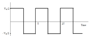
Fig 2: Output waveform of half bridge Inverter
Full Bridge Voltage Source Inverter

Fig 3: Circuit diagram of full bridge voltage source inverter
The above figureshows the power circuit of a full bridge VSI. Thisinverter is similar to the half bridge inverter, however a second leg provides the neutral point to the load. As in the half bridge inverter, both switches Q1and Q2 or Q3 and Q4 in a single leg cannot be on simultaneously because a short circuit across the dc link voltage source Vdc would be occurred. In a full bridge inverter, there are four defined (states 1, 2, 3, and 4)switching states as shown in Table below. The undefined condition should be avoided so as to be always capable of defining the AC output voltage. It can be observed that the AC output voltage can acquire values up to the DC link value Vdc which is twice that obtained with half bridge voltage source inverter. Output voltage is denoted as VAB taken from the load.
The single-phase full bridge is similar to that of two half bridge circuits sharing the same DC bus. The full bridge circuit has two pole-voltages (VAO and VBO), which are similar to that of single phase inverter. Both voltages (VAO and VBO) of the full bridge circuit are square waves but they will have some phase difference.
State | Switching state | Output Voltage | ||
VAO | VBO | VAB | ||
1 | Q1 and Q4 are ON | Vdc/2 | - Vdc/2 | Vdc |
2 | Q2 and Q3 are ON | - Vdc/2 | Vdc/2 | - Vdc |
3 | Q1 and Q3 are ON | Vdc/2 | Vdc/2 | 0 |
4 | Q2 and Q4 are ON | - Vdc/2 | - Vdc/2 | 0 |
State 1
In this state, the power switches Q1 and Q4 are in conduction mode andremaining switches are OFF condition. By using Thevenin’s analysis, polevoltages at ‘A’ and ‘B’ are(VAOand VBO) measured and the output voltage is VAB=VAO-VBO=VDC.
State 2
In this state, the power switches Q2 and Q3 are in conduction modeand remaining switches are in OFF condition. Pole voltages at ‘A’ and ‘B’ aremeasured from the load and the output voltage is determined by VAB=VAO-VBO= -VDC.
State 3
In this state, the power switches Q1and Q3 are in conduction mode andremaining switches are in OFF condition. Voltages at nodes ‘A’ and ‘B’ aremeasured and the output voltage VAB=VAO-VBO= 0
State 4
In this state, the power switches Q2 and Q4 are in conduction modeand remaining switches are in OFF condition. Pole voltages at ‘A’ and ‘B’ aremeasured and a load voltage is calculated as VAB=VAO-VBO= 0

Fig 4: Output voltage waveform of full bridge inverter
The waveform indicates the representation of two pole voltages and loadvoltage wave forms of a full bridge single phase inverter. During the timeperiod (0 to t), switches Q1 and Q4 are ON, and in which pole voltages are measured as
VAO=Vdc/2 and VBO=- Vdc/2.
Then output voltage (load voltage) is given by
VAB = VAO – VBO = Vdc/2 + Vdc/2 = Vdc
Similarly, output voltage can be found for next three intervals.
Square wave operation of the inverter
A single-phase square wave type voltage source inverter produces square shaped output voltage for a single-phase load. Such inverters have very simple control logic and the power switches need to operate at much lower frequencies. Power circuits of half wave and full wave bridge inverters are redrawn in Fig(a) and (b) below.

Fig 5(a) single phase half wave bridge VSI, Fig 5(b) single phase full wave bridge VSI
Here we both circuits are analysed under the assumption of ideal circuit conditions. Means it is assumed that the input dc voltage (Edc) is constant and the switches are lossless. In half bridge topology the input dc voltage is split in two equal parts through an ideal and loss-less capacitive potential divider.
The half bridge topology consists of one leg (one pole) of switches whereas the full bridge topology has two such legs. Each leg of the inverter consists of two series connected electronic switches shown within dotted lines in the figures.
Each of these switches consists of an IGBT type controlled switch across which an uncontrolled diode is put in anti-parallel manner. These switches are capable of conducting bi-directional current but they need to block only one polarity of voltage. The junction point of the switches in each leg of the inverter serves as one output point for the load.
In half bridge topology the single-phase load is connected between the mid-point of the input dc supply and the junction point of the two switches (in Fig. (a) These points are marked as ‘O’ and ‘A’ respectively).
For ease of understanding, the switches Sw1 and Sw2 may be assumed to be controlled mechanical switches that open and close in response to the switch control signal.
Now, if the switches Sw1 and Sw2 are turned on alternately with duty ratio of each switch kept equal to 0.5, the load voltage (VAO) will be square wave with a peak-to-peak magnitude equal to input dc voltage (Edc).
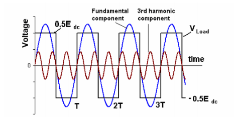
Fig 6: Output voltage of half bridge inverter
The above Fig. Shows a typical load voltage waveform output by the half bridge inverter. VAO acquires a magnitude of +0.5 Edc when Sw1 is on and the magnitude reverses to -0.5 Edc when Sw2 is turned on.
The two switches of the inverter leg are turned on in a complementary manner. For a general load, the switches should neither be simultaneously on nor be simultaneously off. Simultaneous turn-on of both the switches will amount to short circuit across the dc bus and will cause the switch currents to rise rapidly.
For an inductive load, containing an inductance in series, one of the switches must always conduct to maintain continuity of load current.
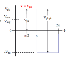
Figure 7. Square Wave
As the name implies, Vavg is calculated by taking the average of the voltage in an appropriately chosen interval. In the case of symmetrical waveforms like the square wave, a quarter cycle faithfully represents all four quarter cycles of the waveform. Therefore, it is acceptable to choose the first quarter cycle, which goes from 0 radians (0°) through π/2 radians (90°).
As with the Vrms formula,
Vavg = 1/π/2  . d
. d = 2/ π . Vpk
  | 0π/2
= 2/π .Vpk (π/2 -0) = Vpk
So, Vavg = Vpk
There are many inverter topologies but output current distortion and efficiency are the two main parameters for the selection of inverters. The unipolar and bipolar inverters uses SPWM (Sinusoidal Pulse Width Modulation) technique.

Fig 8: Single phase H-bridge Inverter
The output waveform (VAB) of switches between positive and negative dc voltages this scheme is called bipolar PWM. The unipolar modulation normally requires two sinusoidal modulating waves’ vm and vm- which are of same magnitude and frequency but 1800 out of phase.
The H-Bridge inverter topologies (both unipolar and bipolar) are made up of power electronic switches and are fed with constant amplitude pulses with varying duty cycle for each period. The SPWM pulses are generated by comparison of two waves- a carrier wave, which is triangular in this case and a modulating reference wave whose frequency is the desired frequency, which is sinusoidal in this case.
This pulse width modulation inverter is characterized by simple circuitry and rugged control scheme that is SPWM technique to obtain inverter output voltage control and to reduce its harmonic content.
Bipolar PWM inverter
In the above fig, the upper and the lower switches in the same inverter leg work in a complementary manner with one switch turned on and other turned off. Thus we need to consider only two independent gating signals vg1 and vg3 which are generated by comparing sinusoidal modulating wave vm and triangular carrier wave vcr. The inverter terminal voltages are obtained denoted by VAN and VBN and the inverter output voltage VAB = VAN-VBN. Since the waveform of VAB switches between positive and negative dc voltages this scheme is called bipolar PWM.

Fig 9: Waveform of Bipolar modulation scheme
Unipolar pwm inverter
The unipolar modulation normally requires two sinusoidal modulating waves’ vm and -vm which are of same magnitude and frequency but 1800 out of phase. The two modulating wave are compared with a common triangular carrier wave vcr generating two gating signals vg1 and vg3 for the upper two switches S1 and S3.
It is observed that the upper two devices do not switch simultaneously, which is distinguished from the bipolar PWM where all the four devices are switched at the same time. The inverter output voltage switches between either between zero and +Vd during positive half cycle or between zero and –Vd during negative half cycle of the fundamental frequency thus this scheme is called unipolar modulation. The unipolar switched inverter offers reduced switching losses and generates less EMI.
On efficiency grounds, it appears that the unipolar switched inverter has an advantage.
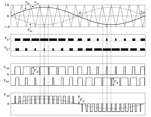
Fig 10: Waveform of Unipolar modulation scheme
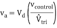
Modulation index is the ratio of peak magnitudes of the modulating waveform and the carrier waveform. It relates the inverter’s dc-link voltage and the magnitude of pole voltage (fundamental component) output by the inverter.
In a pulse width modulated inverter the desired sine-wave output (the modulation) is modulated onto a high frequency square wave (the carrier). This can be done using a high speed digital signal processor but the traditional approach using a Comparator to perform the modulation is perhaps easier to understand.

The amplitude modulation index is defined as:

This will typically be less than one. An amplitude modulation index of more than 1 is possible but this leads to distortion of the output sine wave and in the extreme leads to a square wave output.
When V^control is above V^tri the output is +Vd. When V^controll is below V^tri the output is –Vd. The average output voltage (for this small increment of time) can be
V0=Vd.ma
References:
- Fundamentals of Power Electronics Book by Robert Warren Erickson
- Power Electronics: Principles and Applications Book by Joseph Vithayathil
- Introduction to power electronics Book by Denis Fewson
- R. W. Erickson and D. Maksimovic, “Fundamentals of Power Electronics”, Springer Science & Business Media, 2007.
- L. Umanand, “Power Electronics: Essentials and Applications”, Wiley India, 2009.


