Unit-1
Microprocessor evolution and types
The microprocessor has become a more essential part of many gadgets. The evolution of microprocessor was divided into five generations such as first, second, third, fourth, and fifth-generation and the characteristics of these generations are discussed below.
First Generation Microprocessors
The first-generation microprocessors were introduced in the year 1971-1972. The instructions of these microprocessors were processed serially, they fetched the instruction, decoded and then executed it. When an instruction of the microprocessor was finished, then the microprocessor updates the instruction pointer & fetched the following instruction, performing this consecutive operation for each instruction in turn.
Second Generation Microprocessors
In the year 1970, a small number of transistors were available on the integrated circuit in the second-generation microprocessors. Examples of the second-generation microprocessors are 16-bit arithmetic 7 pipelined instruction processing, MC68000 Motorola microprocessor. The second generation of the microprocessor is defined by overlapped fetch, decode, and execute the steps. When the first generation is processed in the execution unit, then the second instruction is decoded and the third instruction is fetched.
Third Generation Microprocessors
The third-generation microprocessors were introduced in the year 1978, as denoted by Intel’s 8086 and the Zilog Z8000. These were 16-bit processors with a performance like mini computers. These types of microprocessors were different from the previous generations of microprocessors in that all main workstation industrialists began evolving their own ISC based microprocessor architectures.
Fourth Generation Microprocessors
As many industries converted from commercial microprocessors to in house designs, the fourth-generation microprocessors are entered with outstanding design with a million transistors. Leading-edge microprocessors like Motorola’s 88100 and Intel’s 80960CA could issue & retire more than one instruction per clock cycle.
Fifth Generation Microprocessors
Fifth-generation microprocessors employed decoupled superscalar processing, and their design soon exceeded 10 million transistors. In the fifth generation, PCs are a low-margin, high volume business conquered by a single microprocessor.
Types
4-bit Microprocessor
The INTEL 4004/4040 was invented in the year 1971 by Stanley Mazor & Ted Hoff. The clock speed of this microprocessor is 740 KHz.
8-bit Microprocessor
- The 8008 processor was invented in the year 1972. The clock speed of this microprocessor is 500 KHz and instruction per second is 50K
- The 8080 microprocessors were invented in the year 1974. The clock speed is 2 MHz The number of transistors used is 60k and instruction per second is 10 times quicker as compared with 8008 processor.
- The 8085 microprocessors was invented in the year 1976. The clock speed is 3 MHz The number of transistors used is 6,500 and instruction per second is 769230. The number of pins of this microprocessor is 40
16-bit Microprocessor
- The 8086 microprocessor was invented in the year 1978. The clock speed is 4.77, 8 & 10 MHz. The number of transistors used is 29000 and instruction per second is 2.5 Million. The number of pins of this microprocessor is 40
- The 8088 microprocessor was invented in the year 1979 and instruction per second is 2.5 Million
- The microprocessors like 80186 or 80188 were invented in the year 1982. The clock speed is 6 MHz
64-bit Microprocessor
- The INTEL core 2 microprocessor was invented in the year 2006. The clock speed is 1.2 GHz to 3 GHz. The number of transistors used is 291 Million and instruction per second is 64 KB of L1 cache for each core 4 MB of L2 cache.
- The i3, i5, i7 microprocessors were invented in the years 2007, 2009, 2010 2. The clock speed is 2GHz to 3.3GHz, 2.4GHz to 3.6GHz & 2.93GHz to t 3.33GHz.
Key takeaways
The microprocessor is clock driven sequential device. There are 8-bit, 16-bits, 64-bits of microprocessors.
Operations of 8085 Microprocessor
It performs all arithmetical and logical operations like add, subtract, AND, OR etc. The temporary registers and accumulators hold the information throughout the operations and the result is stored in the accumulator. The different flags are arranged or rearranged on the basis of result.
Flag Registers
It is an 8 bit register. They are of five types namely sign, zero, auxiliary carry, parity and carry.
Control and Timing Unit
It coordinates with all the processes of the microprocessor by the clock and provides the control signals required for communication between the microprocessor and peripherals. It is used to control the internal as well as external circuits.
- Decoder and Instruction Register, when an order is received from memory which is located in the instruction register, it is encoded & decoded into various device cycles.
Register Array
The general-purpose registers are classified into several types such as B, C, D, E, H, & L. They are 8-bit registers. The register pairs are BC, DE & HL.
- Special Purpose Registers
These registers are of four types namely program counter, stack pointer, increment or decrement register, address or data buffer.
Program Counter
It is a 16 bit register. It is used to store data, memory information etc. whenever memory is incremented, the PC then points to the next location.
Stack Pointer
It is a 16 bit register. It always points to stack which can be incremented or decremented by PUSH and POP instruction.
Increment or Decrement Register
It is an 8-bit register which can be increased or decreased by one. It is useful for incrementing or decrementing program counters as well as stack pointer register content with one. This operation can be done on any memory location or any kind of register.
Address Bus and Data Bus
Data bus carries the data required to be stored. It is bidirectional. Address bus carries the location to where the data should be stored and it is unidirectional. It is used to transfer the data & address.
|
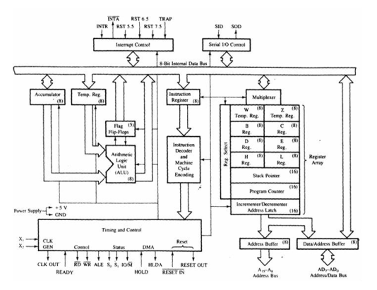
Fig.1: Architecture of 8085 (ref 1)
Key takeaway
It includes the timing & control unit, Arithmetic and logic unit, decoder, instruction register, interrupt control, a register array, serial input/output control and the central processing unit.
1.3.1 Addressing modes
Addressing modes in 8085 is divided into 5 groups −
Here, the 8/16-bit data is specified in the instruction itself as one of its operand.
Example: MVI B, 40F means 40F is copied into register B.
Here, the data is copied from one register to another.
Example: MOV B, A: means data in register A is copied to register B.
Here, the data is directly copied from the given address to the register.
Example: LDB 5008H: means the data at address 5008H is copied to register B.
Here, the data is transferred from one register to another by using the address pointed by the register.
Example: MOV B, K: means data is transferred from the memory address pointed by the register K to the register B.
Here, it doesn’t require any operand; the data is specified by the opcode itself.
Example: CMP.
Key takeaways
There are 5 addressing modes. Immediate, Direct, Indirect, Register and Implied addressing modes.
1.3.2 Interrupts
Interrupts are the signals generated by external devices requesting the microprocessor to perform a certain task. There are 5 types of interrupt. They are TRAP, RST 7.5, RST 6.5, RST 5.5, and INTR.
1.3.3 Data transfer schemes
|
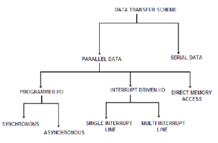
Fig.2: Data transfer schemes (Ref 3)
- Interruption can be done at the time of executing program by the virtue of the program by an Input Output device.
- It can also be done by the method as per the working of the processor.
- The data transfer schemes wants sending information to the processor, rather than receiving information from the processor because sending and receiving information plays a vital role for executing the entire program.
- The communication is not done directly with the Input Output device. It is carried out systematically with the help of Input Output device by the virtue of an Input Output port. The data transfer schemes are as follows:
- Serial data transfer scheme
- Parallel data transfer scheme
- Programmed I/O Data Transfer
- Interrupt Driven I/O data Transfer
- Direct memory access data transfer
Key takeaway
The data transfer schemes wants sending information to the processor, rather than receiving information from the processor because sending and receiving information plays a vital role for executing the entire program.
The 8085-instruction set can be classified into the following five categories:
Data Transfer (copy) Instructions
These instructions perform the following six operations:
Load 8-bit number in a register.
Load 16-bit number in a register pair.
Copy from register to register.
Copy between register and memory.
Copy between I/O and accumulator.
Copy between registers and stack memory.
MVI R, 8-bit
MOV Rd, Rs
LXI Rp, 16-bit
OUT 8-bit
IN 8-bit
LDA 16-bit
STA 16-bit
LDAX Rp
STAX Rp
MOV R, M
Arithmetic Instructions
The frequently used arithmetic operations are: Add, Subtract, Increment (add 1), Decrement (subtract 1)
ADD R
ADI 8-bit
ADD M
SUB R
SUI 8-bit
SUM M
INR R
INR M
DCR R
DCR M
INX Rp
DCX Rp
Logical and Bit Manipulation Instructions
These instructions include the following operations: AND, OR, X-OR, Compare, Rotate bits
ANA R
ANI 8-bit
ANA M
ORA R
ORI 8-bit
ORA M
XRA R
XRI 8-bit
XRA M
CMP R
CPI 8-bit
Branching Instructions
The following instructions change the program sequence.
JMP 16-bit
JZ 16-bit
JNZ 16-bit
JC 16-bit
JNC 16-bit
CALL 16-bit
RET
Miscellaneous Instructions
There are a number of instructions related with data transfer among the register, the stack operation instructions and interrupt operations of 8085 MP which are kept in this group. They are:
PUSH, POP
EI, DI
Machine Control Instructions
These instructions affect the operation of the processor.
Data Flow
Microprocessor consists of an ALU, register array, and a control unit. ALU performs arithmetical and logical operations on the data received from the memory or an input device. Register array consists of registers identified by letters like B, C, D, E, H, L and accumulator. The control unit controls the flow of data and instructions within the computer.
Key takeaway
Instructions are the codes given to the microprocessor by the user in order to perform various operations. They can be arithmetical, logical, machine control etc.
- Timing diagram helps to understand the working of any system step by step and working of each instruction, its decoding, fetching and execution.
- It is the graphical representation with respect to time.
- It represents the clock cycle with duration, delay, content of address bus and data bus, type of operation w.r.to Read/write/status signals.
Important terms used
Instruction cycle: It is defined as the number of steps required by the CPU to complete the process which includes fetching, decoding and execution of one instruction. They are carried out in synchronization with the clock pulse.
Machine cycle: It is the time required by the microprocessor to complete the operation of accessing the memory or I/O devices. Here, operations like opcode fetch, memory read, memory write, I/O read and I/O write can be performed.
T-state: Each clock cycle is known as T-state.
Rules to identify number of machine cycles in an instruction:
If an addressing mode is direct, immediate or implicit then
No. of machine cycles = No. of bytes.
If the addressing mode is indirect then
No. of machine cycles = No. of bytes + 1.
Add +1 to the No. of machine cycles if it is memory read/write operation.
If the operand is 8-bit or 16-bit address then,
No. of machine cycles = No. of bytes +1.
These rules are applicable to 80% of the instructions of 8085.
|
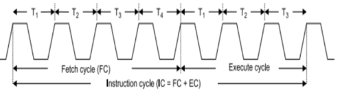
Fig.3: Timing Diagram
Fetch cycle
|
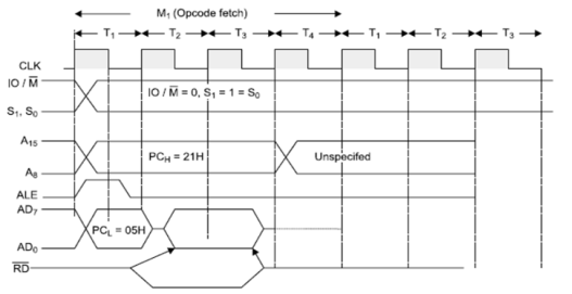
Fig.4: Fetch Cycle
- The microprocessor requires instructions to perform any particular task. In order to perform these tasks, it utilizes Opcode which is a part of an instruction which provides detail to the microprocessor.

 During T1 state, microprocessor uses IO/M, S0, S1 signals are used to instruct the microprocessor to fetch opcode. Thus when IO/M =0 and S0=S1= 1, it indicates opcode fetch operation. During this operation 8085 transmits 16-bit address and also uses ALE signal for address latching.
At T2 state, microprocessor uses read signal and make data ready from that memory location to read opcode from memory and at the same time program counter is incremented by 1 and points next instruction to be fetched. In this state microprocessor also checks READY input signal, if this pin is at low logic level ie. '0' then microprocessor adds wait state immediately between T2 and T3.
At T3 state, microprocessor reads the opcode and stores it into instruction register to decode it further. At T4 state, the microprocessor performs internal operation like decoding opcode and providing necessary actions. The opcode is decoded to know whether T5 or T6 states are required or not for next operation.
Read Cycle
Memory read and I/O read
|
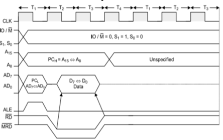
Fig.5: Memory read Cycle
- It fetches one byte from the memory at a time.
- It requires 3 T-States.
- It is used to fetch operand or data from the memory.
- During T1 state, A8-A15 contains higher byte of address, ALE is high therefore lower byte of address A0-A7 is selected from the multiplexed lines AD0-AD7.
 Since it is a memory ready operation, IO/M =0.
 During T2state, ALE = 0, RD = 0 and address is removed from AD0-AD7 and data D0-D7 appears on the lines AD0-AD7.
- During T3 state, data remains on AD0-AD7 till , RD = 0.
I/O Read
|
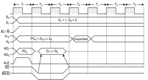
Fig.6: I/O read Cycle


 It is used to fetch one byte from an IO port at a time.
It requires 3 T-States.
During T1 state, the lower Byte of IO address is copied into higher order address bus A8-A15.
ALE = 1 and AD0-AD7 contains address of IO device.
IO/M = 1 as it is an IO operation.
During T2 state, ALE = 0, RD = 0 and data appears on AD0-AD7 as input from IO device.
During T3 state, data remains on AD0-AD7 till RD = 0.
Write Cycle
Memory write and I/O write
|
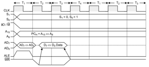
Fig.7 Memory write Cycle


 It is used to send one byte at a time into memory. It requires 3 T-States. During T1 state, ALE = 1 and contains lower address A0-A7 from multiplexed lines AD0-AD7 and A8-A15 contains higher byte of address. As it is memory operation, IO/M = 0. During T2 state, ALE = 0, WR = 0 and address is removed from AD0-AD7 and data appears on AD0-AD7. Data remains on AD0-AD7 till WR = 0.
|
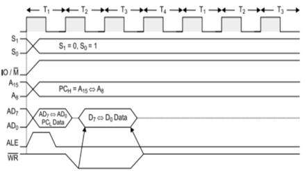
Fig.8: I/O write Cycle


 It is used to write one byte at a time into IO device. It requires 3 T-States. During T1 state, the lower byte of address is copied into higher order address bus A8-A15. ALE =1 and A0-A7 address is selected from the multiplied lines AD0-AD7. As it is an IO operation, IO/M = 1. During T2 state, ALE = 0, WR = 0 and data appears on AD0-AD7 to write data into IO device. During T3 state, data remains on AD0-AD7 till WR = 0.
Key takeaway
- Timing diagram helps to understand the working of any system step by step and working of each instruction, its decoding, fetching and execution.
- It is the graphical representation with respect to time.
- It represents the clock cycle with duration, delay, content of address bus and data bus, type of operation w.r.to Read/write/status signals.
The following figure shows a schematic diagram to interface memory chips and I/O devices to a microprocessor.
|
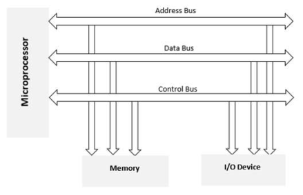
Fig 9 Schematic diagram
When we are executing any instruction, the address of memory location or an I/O device is sent out by the microprocessor. The corresponding memory chip or I/O device is selected by a decoding circuit.
As we know, keyboard and displays are used as communication channel with outside world. Therefore, it is necessary that we interface keyboard and displays with the microprocessor. This is called I/O interfacing. For this type of interfacing, we use latches and buffers for interfacing the keyboards and displays with the microprocessor.
Key takeaway
A microprocessor cannot be connected directly to any device it requires an interface. This interface between the system and the microprocessor is called as interfacing device.
Reference:
1. Gaonkar, Ramesh S , “Microprocessor Architecture, Programming and Applications with 8085”, Penram International Publishing.
2. Ray A K, Bhurchandi K M, “Advanced Microprocessors and Peripherals”, TMH Hall D V, Microprocessor Interfacing’, TMH
3.Liu and, “Introduction to Microprocessor”, TMH
4. Brey, Barry B, “INTEL Microprocessors”, PHI


