Unit - 2
Multistage Amplifiers
Cascading Amplifiers – In most applications, a single transistor will not be able to meet the specifications such as voltage gain, current gain etc.
The transistors are then cascaded i.e., connected in series.

Fig 1 A multistage amplifier is obtained by cascading 3 amplifiers
The meaning of the word “cascading” is to connect a number of amplifier stages to each other with the output of the previous stage to the input of next stage.
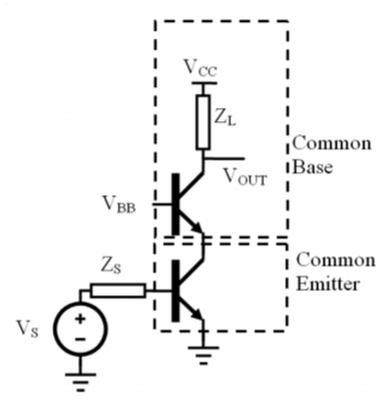
Cascade amplifiers
A CB configuration does not have miller effect because the grounded base shields the collector signal from being fed back to the emitter input. This is the reason why the CB amplifier has high frequency response. The CE gain can be reduced by reducing the load resistance.
A cascade amplifier has moderately high gain, moderately high input impedance and a high output impedance and also high bandwidth.
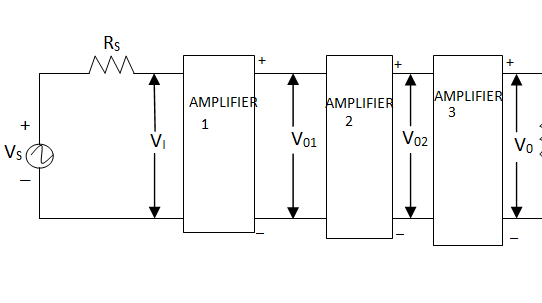
Fig 2 Cascade Amplifier
Key takeaway
For cascade amplifier
CE stage operates at gain=-1, minimising miller loading of input.
CB gives all the voltage gain, acting as transimpedance of value ZL
The cascade has a much higher output impedance (other than ZL) than the CE amplifier (the common emitter Early resistance acts as series-series feedback to the common base with loop gain =gmRCE)
Procedure to analyse the multistage amplifier
b) For current amplifiers start with the first stage and step by step proceed towards the last stage.
- Current gain
- Input resistance
- Voltage gain
- Output resistance
Formulas to be used in each stage-
Current gain: AI = 
Input impendence: AIS = 
Voltage gain: AV = 
Voltage gain: AVS = 
Output admittance: Y0 = 
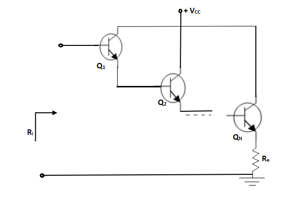
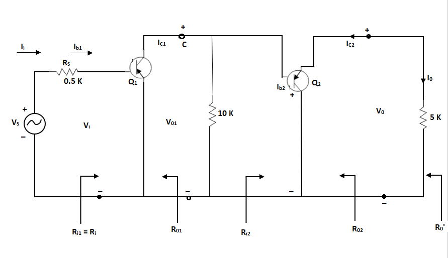
E1) For the circuit shown in below figure find input impendence RI if hie = hre = hoe = 0 and hFe is the same of each of transistor.
S2) Given hie = hre = hoe = 0 and
hFe1 = hFe2 = hFe3 = …... = hFeN = hFe
Check for approximation: hoeRLN’  0.1
0.1
As hoe is zero so all transistor is in valid approximation
Now, Ain = 1 + hFe, RiN = hie + (1 + hFe) RLN
Or RiN = 0 + (1 + hFe) Re
 = (1 + hFe) Re;
 1 + hFe,
 = hie + (1 + hFe)
 Re
Re
 Re
Re
 1 + hFe,
 = hie + (1 + hFe)
 Re
Re
Hence, QN → (1 + hFe) Re
QN-1 →  Re
Re
QN-2 →  Re
Re
Similarly, Q[N-(n-1)] →  Re
Re
Ri1 =  Re (Ans)
Also, AI = AI1 × AI2 × ……. × AIN
Hence, AI = (1 + hFe) N
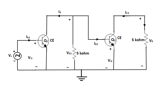
Q2) Determine VONS for the cascade amplifier shown in figure
Use hie = 1 KΩ, hFe = 100, hre = 0, hoe = 0
S2) Given hie = 1 KΩ, hFe = 100, hre = 0, hoe = 0
RC1 = RC2 = 5 KΩ
Q1 → CE
Q2 → CE
The equivalent circuit can be drawn as –
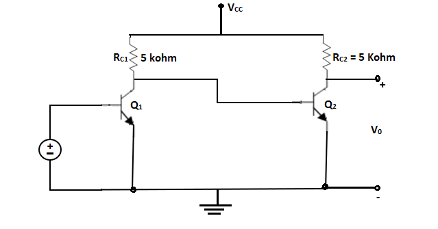
Analysis of Q2 [CE]: Ri2 = 5KΩ hoeRL2 = 0 (approximate analysis)
AI2 =  = -hfe = -100
Ri2 = hie = 1KΩ
AV2 =  =
= 
AV2 = 
Analysis of Q1 [CE]: RL1 = RC1 || Ri2
= 5 K || 1 K = 0.8333 K
hoeRL1 = 0 (approximate analysis)
AI1 =  hFe = -100
Ri1 = hie = 1KΩ
AV1 =  =
= 
AV = 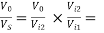 AV1 × AV2
AV = (-500) × (-83.33) = 41650 (Ans)
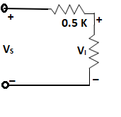
Q3) Find the voltage gain AVS of the amplifier shown.
Assume hie = 1000Ω, hre = 10-4, hFe = 50, hoe = 10-4 A/V
S3) Given: hie = 1000Ω, hre = 10-4, hFe = 50, hoe = 10-4 A/V, RL = 5 KΩ
Q1 → CE, Q2 → CC
For analysis of amplifier, we consider DC supply voltage as ground and modified circuit is given as –
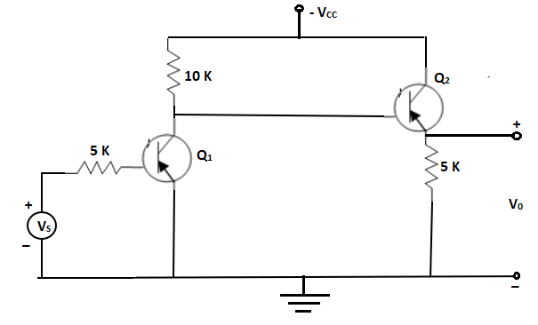
Analysis of Q2 [CC]: hoeRL’ = 10-4 × 5 × 103 = 0.5 > 0.1
approximate analysis is not valid, therefore exact analysis.
AI2 =  =
=  =
=  = 34
= 34
Ri2 = hie + AI2RL’ = 1 + 34 × 5 = 171 KΩ
AV2 =  =
=  0.994
0.994
Analysis of Q1 [CE]:
RL1 = 10 || Ri2 = 9.447 KΩ
hoeRL1 = 10-4 × 9.447 × 103 = 0.9447 > 0.1
so exact analysis
AI1 = 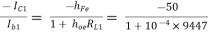 = -25.71
Ri1 = hie + hreAI1RL1 = 1 + 10-4 × (-25.71) × 9.447 = 975.71 Ω
AV1 =  =
= 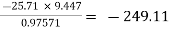
AV = 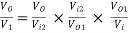
But Vi2 = VO1
AV  = AV1 × AV2
AV = (-249.11) × (0.994) = -247.615
AVS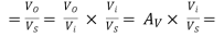 -247.615 × 0.66101 = -163.675 (Ans.)
AI = 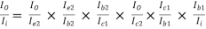
 25.71
25.71
AI2 = 
IO = Ie2, Ib1 = Ii
AI = (-1) × (25.71) × 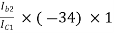
 -0.05524
AI = -25.71 × 34 × 0.05524
= -48.288 (Ans)
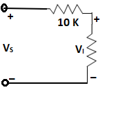
Que.4 For the circuit shown, compute AI, AV, AVS, RI and RO’
Sol: Given: Re = 0.1 KΩ, RL = 3 KΩ RS = 10 KΩ
Q1 → CC, Q2 → CE
AC analysis –
Analysis of Q2 [CE]:
hoe (Re + RL) =  (0.1 + 3) = 0.0775 < 0.1
approximate analysis
AI2 =  = -hFe = -50
Ri2 = hie + (1 + hFe) Re = 1.1 + 51 × 0.1 = 6.2 KΩ
AV2 =  =
=  -24.193
Analysis of Q1 [CE]:
hoe (Re + RL’)
RL’ = Ri2 || 8 K= 3.492 K
 (0.5 + 3.492) = 0.0998 < 0.1
So approximate analysis
AI1 =  = -50
= -50
Ri1 = hie + (1 + hFe) Re = 1.1 + 51 × 0.5 = 26.6 KΩ (Ans)
AV1 =  =
= 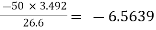
Hence,
AV =  AV1 × AV2 = 158.8 (Ans)
AVS
 =
= 
AVS = 158.8 × 0.7261 = 115.41 (Ans)
AI = 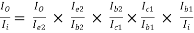
AI1 =  50
50
AI2 = 
AI = (-1) × (50) × 
 -0.5633
AI = 50 × 50 × 0.5633
= 1408.25 (Ans)
RO1 = ∞, RS2 = 8 || ∞ = 8 KΩ
RO2 =∞, RO’ = ∞ || 3 K = 3 K (Ans)
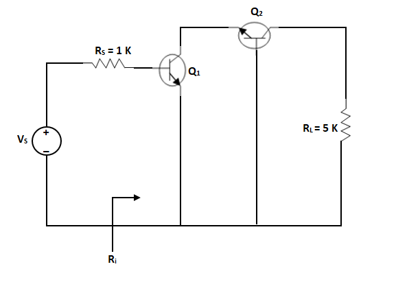
Que 5. Calculate AI, AV, AVS and Ri
Sol – Given: RS = 1 KΩ, RL = 5 KΩ
Amplifier configuration: cascade amplifier [CE – CB]
Analysis of Q2 [CB]:
hoeRL  0.1
0.1
 2.45 × 10⁻³ < 0.1 which is less than 0.1
Approximate analysis:
AI2 =  = -hFb = 0.98
Ri2 = hib = 21.6 Ω
AV2 =  =
=  226.85
Analysis of Q1 [CE]:
RL1 = Ri2 = 21.6 Ω
Checking approximation:
hoeRL1  0.1
0.1
 = 5.4 × 10⁻⁴ < 0.1, which is less than 0.1
So approximate analysis
AI1 =  = -50
= -50
Ri1 = hie = 1.1 KΩ (Ans)
AV1 =  =
= 
Hence,
AV =  AV1 × AV2 = -222.723 (Ans)
AVS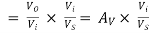 = 0.5238 × (-222.732) = -116.66 (Ans)
[ since  can be given as
 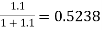 ]
]
AVS = 158.8 × 0.7261 = 115.41 (Ans)
AI =  AI1 × AI2 = -50 × 0.98 = -49 (Ans)
Que 6. For the circuit shown in figure. Calculate the values of Ri, AI, AV and Ro. Assume the following h-parameters for both the transistors.
Hie = 1.1 KΩ, hFe = 50, hre = 2.5 × 10⁻⁴, hoe = 25 μA/V
Sol – Given: hie = 1.1 KΩ, hFe = 50, hre = 2.5 × 10⁻⁴,
hoe = 25 μA/V, RS = 1 KΩ, RE = 1 Ω
Amplifier configuration:
Q1 → CC, Q2 → CC
Analysis of second stage:
Checking approximation: hoeRc2  0.1
0.1
Let us first analyse the second stage. For this stage,
Analysis of Q2 [CE]:
hoeRL2 = 1 × 103 × 25 × 10-6 = 25 × 10-3 [ RC = RE = 1]
which is less than 0.1
approximate analysis:
a) Current gain of second stage (AI2):
AI2  1+ hFe = 1 + 50 = 51 ----------(1)
b) Input resistance
Ri2 = hie + (1 + hFe) RE = 1.1 K + (51 × 1 K)
Ri2 = 52.1 KΩ -----------(2)
c) Voltage gain (AV2):
AV2 =  = 1 -
= 1 -  0.978 -----------(3)
Analysis of the first stage:
The load resistance for the first stage is the input resistance of the second stage Ri2
hoeRi2 = 25 × 10-6 × 52.1 × 10-3 = 1.3
As hoeRi2 > 0.1, we cannot use the approximate analysis. Hence, we will have to use the exact analysis.
a) Current gain (AI1):
We can write the exact equation for the current gain as,
AI1 = 
Substituting the values, we get,
AI1 = 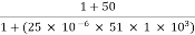 = 22.41 ----------(4)
b) Input resistance (RI1):
Ri1 = hie + AI1Ri2 = 1.1 K + (22.41 × 52.1 K) = 1.169 MΩ ----------(5)
c) Voltage gain (AV1):
AV1 =  = 1 -
= 1 -  0.999 Ω ----------(6)
d) Output resistance (RO1):
RO1 = 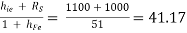 Ω ------------(7)
e) Output resistance of second stage (RO2):
RO2 = 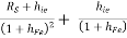
Substituting the values, we get,
RO2 = 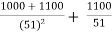 = 22.38 Ω -------------(8)
Combine the result of analysis of stage 1&2:
Overall voltage gain (AV): AV = AV1 × AV2
= 0.978 × 0.999
= 0.977 Ans.
Overall current gain (AI): AI = AI1 × AI2
= 22.41 × 51 = 1142.9 Ans.
Overall input resistance (Ri) = Ri1 = 1.169 MΩ Ans.
Overall output resistance (RO) = RO2 = 22.38 Ω Ans.
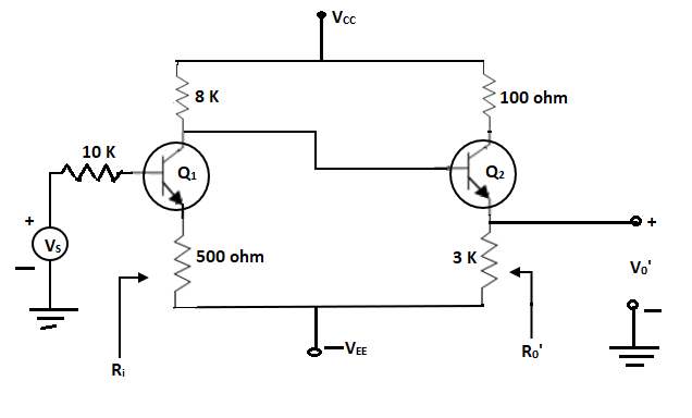
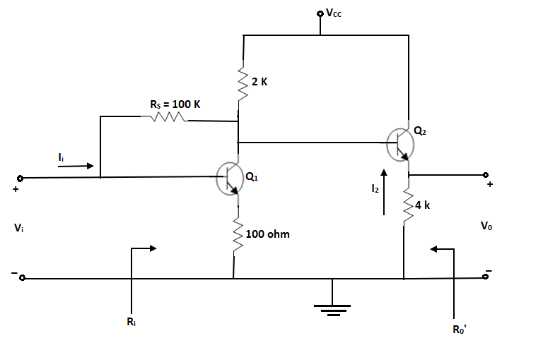
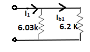
Que 7. For the two-stage cascade, shown calculate AI, AV, Ri and RO’.
Sol – Given: RB = R1 = 100 KΩ, RL = 4 KΩ Re = 0.1 K
Amplifier configuration: Q1 → CE, Q2 → CC with Re
AC analysis: For a.c. analysis of amplifier we consider the d.c. supply as ground and apply Miller’s theorem across feedback resistance (RB = 100 KΩ) then modified circuit is given as:
Analysis of Q2 [CC]:
Check for approximation, hoeR1  0.1
0.1
hoeRL =  × 4 = 0.1
Hence, valid approximation
Approximate analysis:
Current gain:
AI2 =  = 1 + hFe = 1 + 50 = 51
Input Impendence:
Ri2 = hie + (1 + hFe) RL = 1.1 + 51 × 4 = 205.1 KΩ
Voltage gain:
AV2 =  =
=  0.995
0.995
Analysis of Q1 [CE with Re]:
hoe (Re + RL’)
RL’ =  || 2 || Ri2
|AV1| >> 1 for CE,  << 1,
<< 1,  1
1
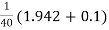
RL1 = 100 || 2 || 205.1 = 1.942 KΩ
Check for approximation hoe (RL’ + Re)  0.1
0.1
 = 0.051 < 0.1
Hence, valid approximation
Approximate analysis:
Current gain:
AI1 =  = -50
= -50
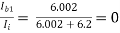
Ri1 = hie + (1 + hFe) Re = 1.1 + 51 × 0.1 = 6.2 KΩ
Voltage gain:
AV1 =  =
= 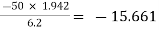
AV =  AV1 × AV2 = -15.661 × 0.995
= - 15.583 (Ans)
Input Impendence:
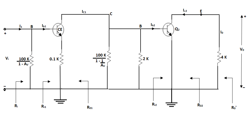
Ri =  || Ri1 = 6.03 K || 6.2 K = 3.05 KΩ (Ans)
Now, RO’ = source resistance for Q2 & RO1 = ∞
RB’ = ∞ ||  || 2K = 1.958 KΩ
From the fig. (a):
RO’ = RO2 || 4 K = 0.060 || 4 = 0.059 KΩ (Ans)
Overall current gain:
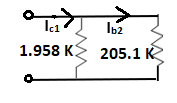
AI = 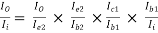
And
AI1 =  50
50
AI2 = 
AI = (-1) × (51) × 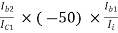
From fig. (b):
From fig. (c):
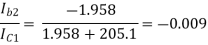
AI = 51 × (- 0.009) × 50 × 0.492 = -11.29 Ans.
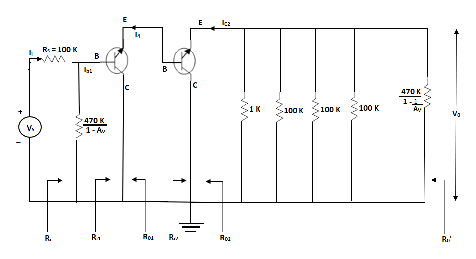
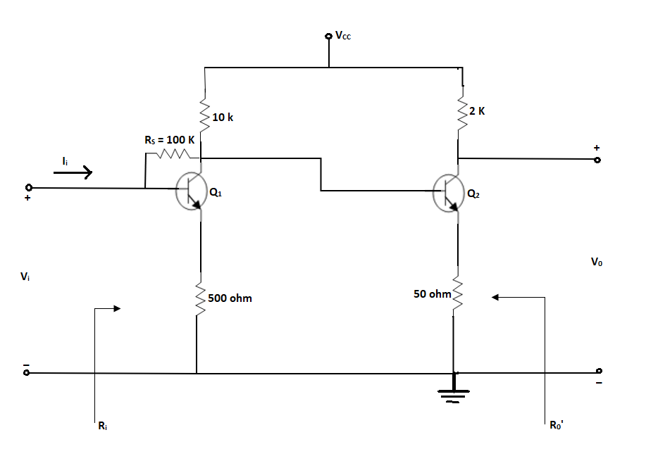
Que 8. For the circuit shown, find AV, AVS, AI =  , Ri and RO
Sol – Given RC = 100 KΩ, Ri = 470 KΩ, R1 = 40 KΩ, R2 = 100 KΩ
Amplifier configuration: Q1 → CC, Q2 → CC with Re
AC analysis: For a.c. analysis of amplifier we consider the d.c. supply voltage as ground and all capacitor as short circuit and apply Miller’s theorem across 470K feedback resistance then modified circuit is given as:
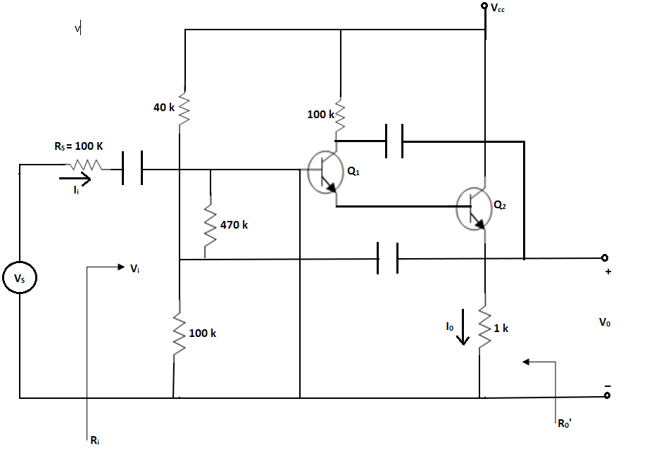
Let us assume AV = 0.96 [Since in CC-CC configuration AV  1]
1]
R2’ = 1K || 40K || 100K || 100K || 
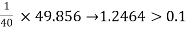
= 1K || 40K || 50K || 11280K = 0.956 KΩ
Analysis of Q2 [CC]:
Check for approximation, hoeRL’  0.1
0.1
0.0239  0.1, which is less than 0.1
Approximate analysis:
AI2 =  = 1 + hFe = 51
Ri2 = hie + (1 + hFe) RL’ = 1.1 + 51 × 0.956 = 49.856 KΩ
AV2 =  =
=  0.9779
Analysis of Q1 [CC]:
RL1 = Ri = 49.856 KΩ
Checking approximation:
hoeRL1  0.1
0.1
 which is greater than 0.1
Exact analysis:
AI1 = 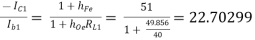
Ri1 = hie + AI1RI1 = 1.1 + 22.70299 × 49.856
= 1132.98 KΩ Ans.
AV1 =  =
= 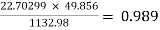
AV = AV1 × AV2 = 0.976 Ans.
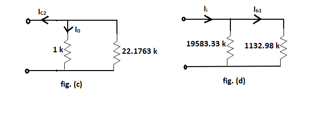
R = 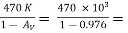 19583.33 KΩ
From Fig. (a):
Ri = R || Ri = 19583.33 K || 1132.98 K = 1071.017 KΩ
AVS = 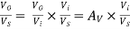 = 0.976 ×
  = 0.8927 Ans.
AI = 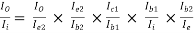
AI 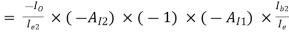
AI = 
AI = 1047.30
RS1 = 100 K || 19583.33 K = 99.491 KΩ
RO1 =  , VO1 = hOe +
 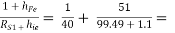 0.532 mʊ
RO1 = 1.8796 KΩ
RS2 = RO1 = 1.8796 KΩ
RO2 = 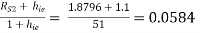 KΩ
KΩ
RO’ = RO2 || RL’ = 0.0584 || 0.956 = 55 Ω Ans.
Que 9. For the two-stage cascade shown, find AI, AV, Ri and RO’.
Sol – Given: RB = 100 KΩ, Re = 0.05 KΩ, RL = 2 KΩ
Amplifier configuration: Q2 → CE with Re, Q1 → CE with Re
AC analysis: For a.c. analysis of amplifier we consider the d.c. supply as ground and apply Miller’s theorem across (RB = 100 KΩ) then modified circuit is given as:
Analysis of Q2 [CE with Re]:
Check for approximation,
hoe (Re+RL)  0.1
0.1
hoe (Re + RL) =  × [0.5 + 2] = 0.05125 < 0.1
Approximate analysis:
AI2 =  = - hFe = -50
Ri2 = hie + (1 + hFe) Re = 1.1 + 51 × 0.05 = 3.65 KΩ
AV2 =  =
=  -27.397
Analysis of Q1 [CE with Re]:
RL’ =  || 10 || Ri2
Assume |AV1| = 1 for CE,
 << 1,
<< 1,  1
1
RL’ = 100 || 10 || 3.65 = 2.604 KΩ
Check for approximation hoe (RL’ + Re)  0.1
0.1
hoe (RL’ + Re) = 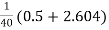 = 0.078 < 0.1
Approximate analysis:
AI1 =  = -50
= -50
Ri1 = hie + (1 + hFe) Re = 1.1 + 51 × 0.5 = 26.6 KΩ
AV1 =  =
= 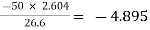
AV =  AV1 × AV2 = (-4.895) × (-27.397)
= 134.108 (Ans)
Ri =  || Ri1 = 16.964 || 26.6 = 10.358 KΩ (Ans)
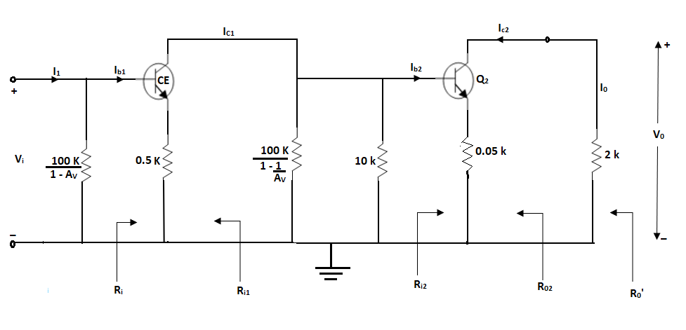
AI = 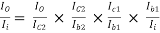
AI1 =  50
50
AI2 = 
AI = (-1) × (50) × 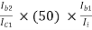
From fig. (b),
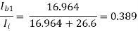
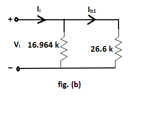
From fig. (d):
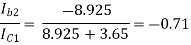
AI = 50 × 0.71 × 50 × 0.389 = 690.475 Ans.
RO2 = ∞, RO’ = 2 || ∞ = 2 KΩ (Ans)
In general, a single stage amplifier is not capable of providing input and output impedances of correct magnitudes. In such cases if more than one amplifier stages are cascaded then the input stage takes cascade of the input impedance while the output stage takes care of the output impedance matching requirements and the middle stages will fulfil the high voltage gain requirements.
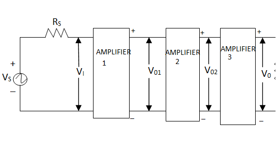
Fig 3 Cascading of Amplifiers
The meaning of the word “Cascading” is to correct a number of amplifier stages to each other with the output of the previous stage to the input of next stage. Thus, a multistage amplifier is obtained by cascading a number of amplifiers.
Thus, cascading is to be done when:
1) The amplification provided by a single stage amplifier is not sufficiently large.
2) The input and output impedances are not of correct value.
Gain of cascaded configuration- The overall gain of the amplifier is given as-
Av 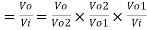
Where:
 Av3 = Voltage gain of amplifier
 = Av2 = Voltage gain of amplifier 2
 = Av1 = Voltage gain of amplifier 1
Therefore Av= Av3×Av2×Av1 voltage
Thus, the overall gain of a cascaded multistage amplifier is equal to the product of the voltage gains of the individual amplifier stages.
Similarly, we can prove that the overall current gain of a multistage amplifier is given by,
AI = AI3 × AI2 × AI1
Where AI = overall current gain
AI1, AI2, AI3 = current gain of individual amplifiers.
For a n-stage cascaded amplifier – In general it is possible to cascade n-number of stages as shown below-
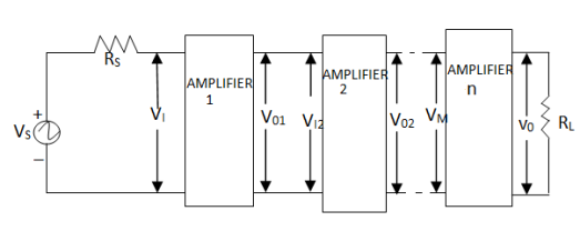
Fig 4 Cascaded amplifiers for gain calculation
All the principles of a 3-stage cascaded amplifiers are applicable to the n-stage cascaded amplifiers as well
Thus, the voltage gain of the overall cascade connection is
Av = Av1.Av2……. Avn
Bandwidth Shrine Rages in Multistage amplifiers-
Let FL (n) be the lower 3db frequency of the “n’’ stage cascaded amplifier and FH (n) be its upper 3db frequency
Bandwidth = FH (n) - FL(n)
Assume that ‘n’ identical stages are connected in cascade. Let all of them identical 3db frequencies “FL” identical values of Av(mid) and Av(low)
Now the overall value of Av(mid) and Av(low) are given by,
Av(mid) = Av1(mid)×Av2(mid)×…. Avn(mid)
Av(mid) = {Av(mid)} n …………. (1)
Similarly, Av(low) = {Av(low)} n ……………. (2)
Dividing equations (2) by (1) we get
 =
= 
=  …………... (3)
Lower 3dB frequency: -
Expression for Av(low) is given by,
Av(low) = 
 =
=  n ……… (4)
At the lower 3dB frequency of the multistage amplifier the value of overall Av(mid) will be 70.7% of the overall Av(mid) as usual.
Let the lower 3dB Frequency of the multistage amplifier be “FL (n)”
At F = FL (n)  =
=  n =
n = 
Therefore 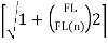 n =
n = 
Squaring both the side, we get


1+ 2 n = 2
Taking the nth root of both the side we get,
1+ 2 = 2 1/n
Therefore  2 = 2 1/n -1
Where FL(n) = Lower 3dB frequency of the cascaded amplifier
FL= Lower 3dB frequency of the single stage amplifier
n= Number of stages connected in cascaded
Equation (V) indicates that with increase in the number of stage “n” the value of the lower 3dB frequency FL(n) increase. This is the effect of cascading on the lower 3dB frequency.
Upper 3dB frequency:
Similarly, we can write down the relation between the upper 3dB frequencies of cascaded multistage amplifier FH(n) and the upper 3dB frequency of single stage FH as,
 =
=  n =
n = 
 n =
n = 
Squaring both the sides

 1+
1+  2 n = 2
Taking the nth root of both sides we get,
1+  2 = 21/n
 2 = 21/n - 1
Taking Square root of both the sides
 =
=  ……………. (6)
Where,
FH (n) = Upper 3dB frequency of cascaded multistage amplifier
FH = Upper 3dB frequency of single stage amplifier
n = Number of identical stages connected in cascaded.
Equation (6) indicates that with increase in the number of stage “n” the value of the upper 3dB frequency FH (n) decreases. This is the effect of cascading on the upper 3dB frequency.
Bandwidth: The bandwidth of a cascaded multistage amplifier having “n” number of stages is given by,
Bandwidth (BW) = FH (n) – FL (n)
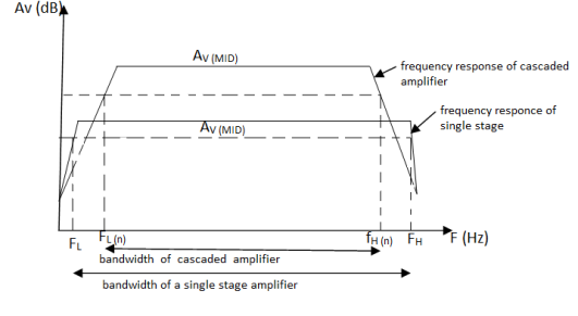
Fig 5: Comparison of bandwidth of the cascaded and single stage amplifier.
The above graph shows that with increase in the number of stages “n” the gain increases but the bandwidth goes on decreasing.
Key takeaway
The cascading is to be done when:
Numerical
Sol- Given: FL(n) = 25 HZ, FH(n) = 16 KHZ n = 3
Lower 3dB frequency, FL for each stage:
Therefore FL(n) 
FL = FL (n) × 
= 25 ×  = 12.75 HZ
Upper 3dB frequency FH for each stage:
Therefore FH(n) = FH 
FH= 
FH=  = 31.38 KHZ
Bandwidth of each stage: BW = FH – FL =31.38 KHZ – 12.75HZ
= 31.37 KHZ
Q2) For identical stages are cascaded. The lower and upper 3dB frequencies of each stage are 40 HZ and 20 KHZ respectively. Calculator the overall bandwidth of the cascaded amplifier
Sol- Given:
FL = 40 HZ, FH = 20 KHZ, n=4
Lower 3dB frequency FL(n):
FL(n) = 
Substitute the values we get,
FL(n) =  = 91.95 HZ
Upper 3dB frequency FH(n):
FH(n) = FH 
Substitute the values, we get
FH(n) = 20×103  = 8.7 KHZ
Overall Bandwidth,
BW = FH(n) – FL(n) = 8.7 KHZ – 91.95 HZ
= 8.6 kHz
Feedback Amplifier is a device that is based on the principle of feedback. The process by which some part or fraction of output is combined with the input is known as feedback.
back to the input.
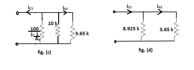
Fig 6 Feedback Network
Amplifier is a device that amplifies the signal. In an ideal amplifier, there exist some important characteristics like voltage gain, input impedance, output impedance, bandwidth etc.
These parameters of an amplifier are controlled by employing a feedback network. Thus, a feedback network is employed in an amplifier to control the gain and other factors of the device.
2.5.1 Classification of Feedback amplifiers
Positive Feedback amplifier– It is a type of an amplifier in which source signal and the feedback signal are in the same phase. Thus, the feedback signal applied increases the strength of the input signal.
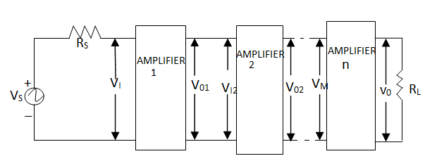
Fig 7 Signal in phase
Negative Feedback amplifier– In this type of amplifier source signal and the feedback signal are out of phase with each other. Thus, the feedback signal applied to decrease the strength of the input signal.

Fig 8 Signal out of phase
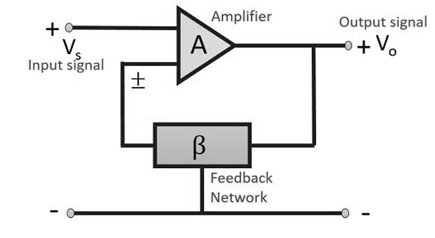
Fig 9 Feedback Amplifier
An input signal Vs is applied to the amplifier with gain A, that produces an amplified signal, Vo.
A portion or fraction of this Vo is then fed to a feedback network having gain β. The output of feedback network is Vf, this signal is then given to summer or a mixer that resultantly produces either sum or difference of two signal depending on their phase relationship.
The gain of an amplifier is given as the ratio of output voltage or current to the input voltage or current.
The gain of the circuit without feedback is given as
A= Vo/Vd -----------------(1)
The gain of feedback network is given as
β = Vf/Vo ----------------(2)
Vd is the mixer output voltage given by
Vd = Vs ± Vf --------------------------(3)
The signal voltage Vs and mixer output voltage Vd will only be equal in a feedback amplifier unless the output is not generated.
From Eq 1 we can write as
Vo = A Vd -----------------------------------(4)
Substituting the value Vd in eq 4
Vo = A [ Vs ± Vf] -------------------------------(5)
From Eq 2
Vf = β Vo ------------------------------------(6)
Substituting the value of Vf in eq 5
Vo = A [ Vs ± β Vo]
Vo = A Vs ± A β Vo
Vo ± A β Vo = A Vs
Vo [1± Aβ] = A Vs
Vo/Vs = A / 1 ± Aβ
Avf = A/ 1 ± Aβ where Vo/Vs = Avf
This is the desired value for the gain of the feedback amplifier.
The gain of an amplifier is always greater than 1. This simply means that some elements are present which increases the gain of the amplifier. That element can be a transistor or a MOSFET.
But a feedback network is always a linear network consisting of RLC elements and it does not contain any such amplification device.
That’s why the value of Vf is always less than Vo.
So, β < 1
In case of a positive feedback the source signal will be in phase with that of the feedback signal.
Thus, the mixer will produce the summation of the two-signal applied to it in case of positive feedback.
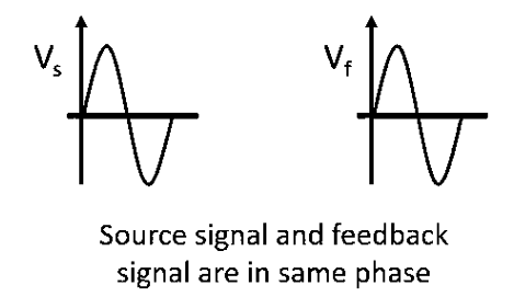
Fig 10 Positive Feedback Amplifier
So, the gain of the amplifier is given as
Avf = A/ 1 - Aβ
This is the gain for a positive feedback amplifier.
The source signal and the feedback signal are out of phase with respect to each other.
Thus, the mixer circuit will resultantly produce the difference between the two signals in case of a negative feedback amplifier.
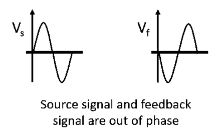
Fig 11 Negative Feedback
So, in this case, the gain of the amplifier is given as
Avf = A / 1+Aβ
For a negative feedback, the value of denominator is always greater than 1, this will decrease the overall gain of the system by the factor 1 +Aβ.
In case of a positive feedback system, the value of denominator is always less than 1, this will resultantly increase the overall gain by 1 – Aβ.
For an ideal system, the gain of the amplifier is infinite. Thus, for a smaller input, we will have a much higher value as output. So, such a large gain is not desirable in the circuit.
The system becomes stable only when its gain is small.
Hence, by decreasing the gain the stability of the system increases and vice-versa.
So, to have a stable system, the gain of the amplifier must be small and it is achieved by employing negative feedback in the circuit.
2.5.2 Properties of negative Feedback amplifiers
The feedback in which the feedback energy i.e., either voltage or current is out of phase with the input and thus opposes it, is called as negative feedback.
In negative feedback, the amplifier introduces a phase shift of 180o into the circuit while the feedback network is so designed that it produces no phase shift or zero phase shift. Thus, the resultant feedback voltage Vf is 180o out of phase with the input signal Vin.
Though the gain of negative feedback amplifier is reduced, there are many advantages of negative feedback such as
2.5.3 Impedance considerations in different configurations
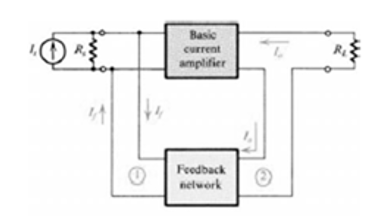
There are four basic feedback amplifiers on the basis of current and voltages as feedback.
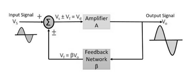
Fig 12 Voltage Series Feedback amplifier
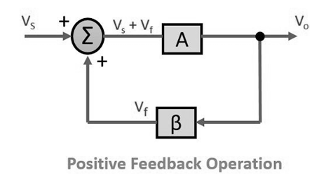
Fig 13 Voltage Shunt Feedback Amplifier
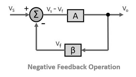
Fig 14 Current Series Feedback Amplifier
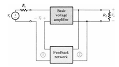
Fig 15 Current Shunt Feedback Amplifier
Key takeaway
An input signal Vs is applied to the amplifier with gain A, that produces an amplified signal, Vo.
A portion or fraction of this Vo is then fed to a feedback network having gain β. The output of feedback network is Vf, this signal is then given to summer or a mixer that resultantly produces either sum or difference of two signal depending on their phase relationship.
The gain of an amplifier is given as the ratio of output voltage or current to the input voltage or current.
The gain of the circuit without feedback is given as
A= Vo/Vd -----------------(1)
The gain of feedback network is given as
β = Vf/Vo ----------------(2)
Vd is the mixer output voltage given by
Vd = Vs ± Vf --------------------------(3)
The signal voltage Vs and mixer output voltage Vd will only be equal in a feedback amplifier unless the output is not generated.
From Eq 1 we can write as
Vo = A Vd -----------------------------------(4)
Substituting the value Vd in eq 4
Vo = A [ Vs ± Vf] -------------------------------(5)
From Eq 2
Vf = β Vo ------------------------------------(6)
Substituting the value of Vf in eq 5
Vo = A [ Vs ± β Vo]
Vo = A Vs ± A β Vo
Vo ± A β Vo = A Vs
Vo [1± Aβ] = A Vs
Vo/Vs = A / 1 ± Aβ
Avf = A/ 1 ± Aβ where Vo/Vs = Avf
This is the desired value for the gain of the feedback amplifier.
The gain of an amplifier is always greater than 1. This simply means that some elements are present which increases the gain of the amplifier. That element can be a transistor or a MOSFET.
But a feedback network is always a linear network consisting of RLC elements and it does not contain any such amplification device.
That’s why the value of Vf is always less than Vo.
So, β < 1
In case of a positive feedback the source signal will be in phase with that of the feedback signal.
Thus, the mixer will produce the summation of the two-signal applied to it in case of positive feedback.
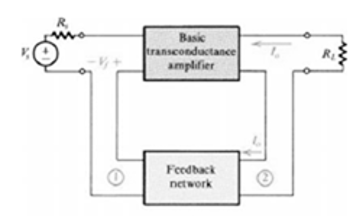
Fig 16 Positive Feedback Amplifier
So, the gain of the amplifier is given as
Avf = A/ 1 - Aβ
This is the gain for a positive feedback amplifier.
The source signal and the feedback signal are out of phase with respect to each other.
Thus, the mixer circuit will resultantly produce the difference between the two signals in case of a negative feedback amplifier.
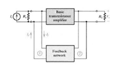
Fig 17 Negative Feedback
So, in this case, the gain of the amplifier is given as
Avf = A / 1+Aβ
For a negative feedback, the value of denominator is always greater than 1, this will decrease the overall gain of the system by the factor 1 +Aβ.
In case of a positive feedback system, the value of denominator is always less than 1, this will resultantly increase the overall gain by 1 – Aβ.
For an ideal system, the gain of the amplifier is infinite. Thus, for a smaller input, we will have a much higher value as output. So, such a large gain is not desirable in the circuit.
The system becomes stable only when its gain is small.
Hence, by decreasing the gain the stability of the system increases and vice-versa.
So, to have a stable system, the gain of the amplifier must be small and it is achieved by employing negative feedback in the circuit.
Key takeaway
For a negative feedback, the value of denominator is always greater than 1, this will decrease the overall gain of the system by the factor 1 +Aβ.
In case of a positive feedback system, the value of denominator is always less than 1, this will resultantly increase the overall gain by 1 – Aβ.
References:
1. “Electronic Devices and Circuit Theory”, Boylestad and Nashelsky, PEARSON
PUBLICATION.
2. “Electronic devices and circuits”, Salivahanan, Suresh Kumar, Vallavaraj,
TMH, 1999
3. “Integrated Electronics, Analog and Digital Circuits and Systems”, J. Millman
and Halkias, TMH, 2000
4. “Micro Electronic Circuits”, Sedra and Smith, Oxford University Press, 2000
5. “Electronic Devices and Circuits”, David A Bell, Oxford University Press, 2000


