Unit 5
Power circuit of single- phase Voltage Source Inverter
Single-phase voltage source inverters (VSIs) can be found as
In Single phase half bridge Two large capacitors are required to provide a neutral point N, such that each capacitor maintains a constant voltage vi=2.
Because the current harmonics injected by the operation of the inverter are low-order harmonics, a set of large capacitors (C+ and C-) is required.
Here both switches S+ and S- cannot be on simultaneously because a short circuit across the dc link voltage source vi would be produced.
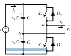
Figure 1. Half bridge single phase VSI
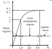
Figure 2. Output
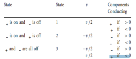
There are two defined (states 1 and 2) and one undefined (state 3) switch state as shown in Table.
In order to avoid the short circuit across the dc bus and the undefined ac output voltage condition, the modulating technique should always ensure that at any instant either the top or the bottom switch of the inverter leg is on.
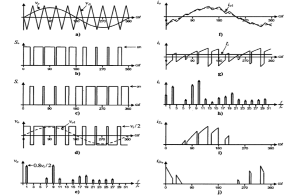
Figure 3. Output
A switching circuit is used in the conversion of DC voltage to an alternating square voltage. One method is the use of inverter bridge known as H-bridge as shown in figure.
The switch symbols are used to represent switching transistors (IGBTs or MOSFETs) or other types of electronic switching devices. In fig (a) S2 and S3 are on for a specified time and S1 and S4 are off.
The direct current is through the load which creates positive output voltage. In figb opposite switches are on and off. The current is in the opposite direction through the load and the output voltage is negative. The complete on/off cycle of the switches produces an alternating square wave.
The transistors are switched by timing control circuit. The harmonic distortion of a typical square wave output is in the range of 45% which can be reduced by filtering out some of the harmonics.
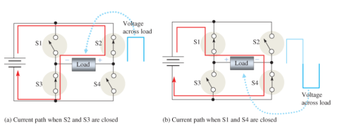
Figure . Current path across the load
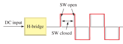
Figure 4. Output voltage
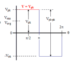
Figure 5. Square Wave
As the name implies, Vavg is calculated by taking the average of the voltage in an appropriately chosen interval. In the case of symmetrical waveforms like the square wave, a quarter cycle faithfully represents all four quarter cycles of the waveform. Therefore, it is acceptable to choose the first quarter cycle, which goes from 0 radians (0°) through π/2 radians (90°).
As with the Vrms formula,
Vavg = 1/π/2  . d
. d = 2/ π . Vpk
  | 0 π/2
= 2/π . Vpk (π/2 -0) = Vpk
So, Vavg = Vpk
Bipolar:
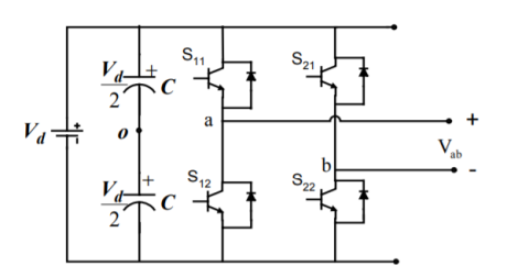
Figure6. Single Phase full bridge Inverter
In this scheme the diagonally opposite transistors S11,S22,S21 and S12 are turned on or turned off at the same time. The output of leg A is equall and opposite to the output of leg B. The output voltage is determined by comparing the control signal Vr and triangular signal Vc as shown in fig(a) to get switching pulses for the devices and the switching pattern as follows:
Vr > Vc s11 is on => Va0 = Vd/2 and S22 is on => Vb0= -Vd/2 ---------(1)
Vr< Vc S12 is on => Va0 = -Vd/2 and S21 is on => Vb0 = Vd/2 ------(2)
Hence
Vbo(t) = Va0(t) --------(3)
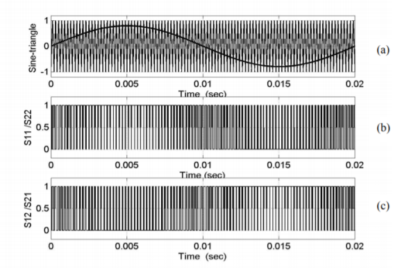
Figure7. Bipolar PWM (a) Sine triangle comparison (b) Switching pulses for s11/s22 (c) Switching pulses for S12/S21
For the bipolar PWM switching scheme there is only one modulation signal and the switches are turned ‘on’ or turned ‘off’ according to the pattern given in Equations (1) and (2). The input dc voltage was 200 V and the modulation index (mi) was taken to be 0.8. The switching frequency for the carrier, which is the triangle, is 10 kHz.
Unipolar
In this scheme the devices in one leg are turned on or off based on the comparison of the modulation signal V with a high frequency triangular wave. The devices in the other leg are turned on or off by the comparison of the modulation signal with the same high frequency triangular wave. Figure show the unipolar scheme for a single –phase full bridge inverter, with the modulation signals for both legs and the associated comparison to yield switching pulses for both the legs. r −Vr In Figure(a) the simulation results show the sine triangle comparison, the switching pulses for S11 and S21 are shown. The switching for the other two devices is obtained as S12 = 1 – S11 and S22 = 1- S21. Figure (b) shows the phase voltages , line to-line voltages obtained from a unipolar PWM scheme , also shown is the load current. The simulation was carried out for an RL load of R = 10Ω and L = 0.125H. The dc voltage is 200 V and the switching frequency is 10kHz. The modulation signal has a magnitude of 0.8, i.e mi = 0.8.
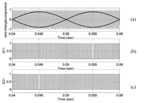
Figure8 (a)
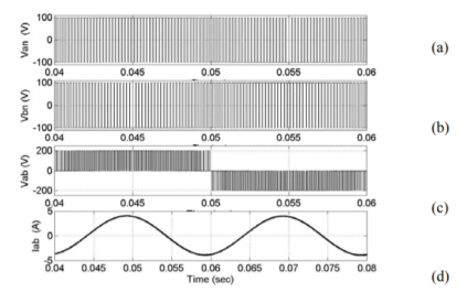
Figure 8(b)
Modulation index is the ratip of peak magnitudes waveform and the carrier waveform. It relates the inverters dc link voltage and the magnitude of pole voltage output by the inverter. Now let  sin(wt) be the modulating signal and let the magnitude of triangular carrier signal vary between the peak magnitudes of triangular carrier signal vary between the peak magnitudes of +
  and -
and -  . The ratio of the peak magnitudes of modulating waveform wave (
  and the carrier wave
  is define as the modulation index.
5.7 Power circuit of three phase voltage source inverter
The circuit diagram of a three-phase inverter is shown below. The main function of this kind of inverter is to change the input of DC to the output of three-phase AC. A basic 3 phase inverter includes 3 single phase inverter switches where each switch can be connected to one of the 3 load terminals.
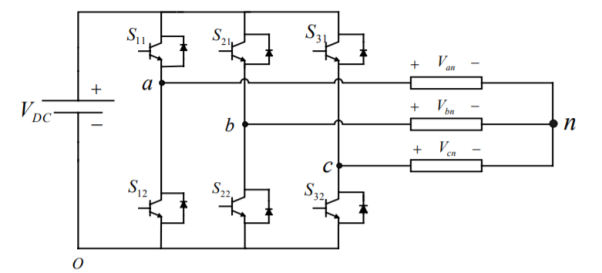
Figure 9. Three Phase Inverter Circuit
Generally, the three arms of this inverter will be delayed with 120 degrees angle to generate a 3 phase AC supply.
The switches used in the inverter have 50% of ratio and switching can be occurred after every 60 degrees angle. The switches like S1, S2, S3, S4, S5, and S6 will complement each other. In this, three inverters with single-phase are placed across a similar DC source. The pole voltages within the three-phase inverter are equivalent to the pole voltages within the half-bridge inverter with a single phase.’
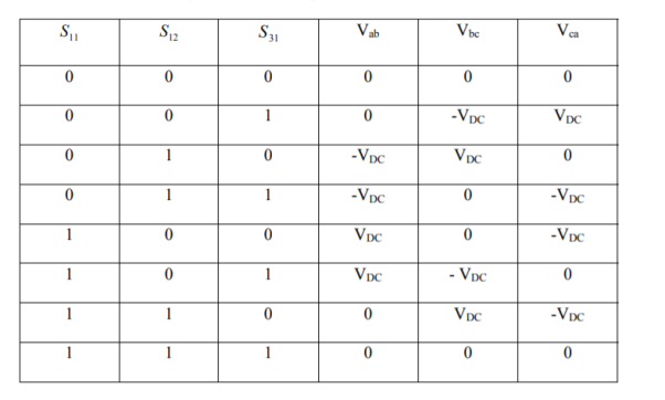
The inverter has eight switch states given in Table 4.1. As explained earlier in order that the circuit satisfies the KVL and the KCL, both of the switches in the same leg cannot be turned ON at the same time, as it would short the input voltage violating the KVL.
Thus, the nature of the two switches in the same leg is complementary.
In accordance to Figure
S11 + S12 = 1
S21 + S22 = 1
S31 + S32=1
Of the eight switching states as shown in Table two of them produce zero ac line voltage at the output. In this case, the ac line currents freewheel through either the upper or lower components. The remaining states produce no zero ac output line voltages. In order to generate a given voltage waveform, the inverter switches from one state to another. Thus, the resulting ac output line voltages consist of discrete values of voltages, which are -VDC, 0, and VDC.
The selection of the states in order to generate the given waveform is done by the modulating technique that ensures the use of only the valid states.
VDC/2 (S11 – S12) = Van + Vno
VDC/2 (S21 – S22) = Vbn + Vno
VDC/2(S31-S32) = Vcn + Vno
In this conduction mode, each device will be in conduction with 180° where they are activated at intervals with 60°. The output terminals like A, B, and C are connected to the star or 3 phase delta connection of the load.
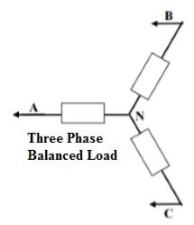
Figure 10.Balanced Load
The balanced load for three phases is explained in the following diagram. For 0 to 60 degrees, the switches like S1, S5 & S6 are in conduction mode. The load terminals like A & C are linked to the source on its positive point, whereas the B terminal is associated with the source on its negative point. Furthermore, the R/2 resistance is available among the two ends of neutral & the positive whereas R resistance is available among the neutral & the negative terminal.
In this mode, the voltages of load are given in the following.
VAN = V/3,
VBN = −2V/3,
VCN = V/3
The line voltages are given in the following.
VAB = VAN − VBN = V,
VBC = VBN − VCN = −V,
VCA = VCN − VAN = 0
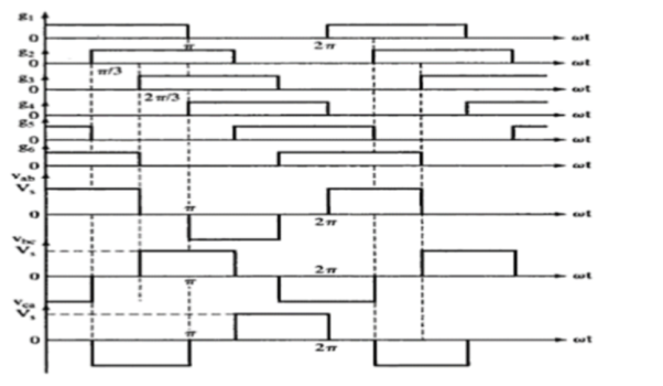
Figure 11. Output waveforms
120° Conduction Mode
In this type of conduction mode, every electronic device will be in a conduction state with 120°. It is apt for a delta connection within a load as it results within a six-step kind of waveform across one of its phases. So, at any instant, only these devices will conduct every device that will conduct at 120° only.
The connection of ‘A’ terminal on the load can be done through the positive end whereas the B terminal can be connected toward the negative terminal of the source. The ‘C’ terminal on the load will be in conduction is known as the floating state. Also, the phase voltages are equivalent to the voltages of load which is given below.
Phase voltages are equal to line voltages, so
VAB = V
VBC = −V/2
VCA = −V/2
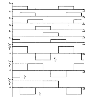
Figure 12. Output Waveforms
The selection of the states in order to generate the given waveform is done by the modulating technique that ensures the use of only the valid states.
Vdc/ 2 (S11 – S12) = Van + Vno ---------------------------(1)
Vdc/2 (S21 – S22) = Vbn + Vno --------------------------------(2)
Vdc/2 (S31-S32) = Vc + Vno -------------------------------------------------(3)
Expressing the Equations from (1) to (3)in terms of modulation signals and making use of conditions to give
Vdc/2 (M11) = Van + Vno -----------------------------------------------(4)
Vdc/2 (M21) = Vbn + Vno --------------------------------------------(5)
Vdc/2 (M31) = Vcn + Vno ---------------------------------(6)
Adding the Equations from (1) to (3) together gives (7) as
Vdc/3 (2S11 – S21-S31) = Van
Vdc/2 (2S21-S21-S31) = Vbn
Vdc/3 ( 2S31-S21-S11) = Vcn
Using sinusoidal reference signal will produce varied width pulses that proportional to the amplitude of the sine wave as shown in Figure. In this technique, the lower order harmonics of the modulated voltage wave are greatly reduce. The rms value of the output voltage of the depends on the widths of the pulses (δm). These widths depend on the modulation index M which controls the output voltage of the inverter.
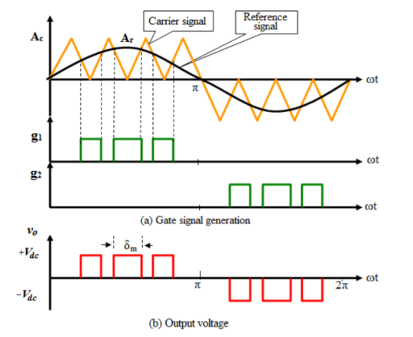
Figure 13.Sinusodial pulse width modulation
The magnitude of the fundamental component of the output voltage is clearly proportional to the modulation index Ar /Ac . But the highest practical value of M is unity. If Ar ˃ Ac the output voltage waveform vo(ωt) approaches a rectangular form and undesirable low frequency harmonics such as the third , fifth and seventh harmonics are introduced and intensified.
The rms output voltage is
Vo = Vdc 
 / π and the co-efficient of the Fourier series of the output voltage will be
Bn =  / n π sin n δ/4 [ sin αm + 3δm/4) – sin n (π + αm + δm/4)
References:


